 >
>


Product overview of the TZMC4V7-GS08 Vishay Zener diode
The TZMC4V7-GS08 Zener diode from Vishay General Semiconductor exemplifies refined engineering within compact voltage regulation components. Harnessing a nominal Zener voltage of 4.7 V and handling up to 500 mW of power dissipation, the device leverages the breakdown mechanism intrinsic to semiconductor PN junctions, enabling stable voltage clamping even under variable load or input conditions. Its ±5% tolerance in Zener voltage is achieved through controlled doping profiles and wafer-level process calibration, minimizing parameter drift over temperature cycles and operational stress.
Encapsulated in a SOD-80 (MiniMELF) package, the TZMC4V7-GS08 addresses the persistent demand for high component density on PCBs without compromising electrical integrity or ease of automated assembly. The low profile and robust surface-mount form factor reduce parasitic effects and facilitate multi-layer board integration—a decisive factor in mixed analog-digital designs where stray capacitance and inductance can degrade reference circuit stability.
In voltage reference generation for precision analog front-ends, the device's predictable I-V characteristics ensure repeatable operation across batches. For input protection, the fast response and low leakage current guard sensitive transceiver or microcontroller inputs against voltage spikes, thereby extending system reliability even under transient-inducing EMC environments. Experience confirms that strategic placement of the TZMC4V7-GS08, particularly proximal to noise-prone interfaces, mitigates risks of latch-up or signal degradation in automotive and industrial control blocks.
The diode's behavior under pulse loading and temperature variation demonstrates robust thermal cycling resilience, a consequence of optimized die-attach materials and interconnect geometry within the MiniMELF structure. Integration into telecom node line interfaces benefits notably from the device’s rapid dynamic clamping capabilities, offering consistent overvoltage suppression during fast signal transitions, while its small footprint permits tight channel spacing.
Subtle design advantages emerge in multi-voltage rail architectures, where the ability to implement discrete, low-loss voltage limits supports clean segmentation between analog supplies and digital logic, reducing error propagation. The TZMC4V7-GS08’s repeatable breakdown threshold, paired with measured leakage control, enables cost-efficient modular designs in instrumentation and sensor clusters without the systematic issues often found in less rigorously characterized Zener diodes.
Continuous feedback from in-field deployments highlights the diode’s contribution to long-term operational stability, especially in thermal cycling and vibration-intensive settings typical of transport and automated manufacturing. The device’s engineered margin against surge and ESD events provides a practical edge, aiding rapid prototyping and system tuning cycles necessary for resilient electronic control platforms.
Technical features and device capabilities of the TZMC4V7-GS08
Technical exploration of the TZMC4V7-GS08 reveals a diode optimized for transient voltage suppression and precision clamping tasks. Central to its architecture is the sharply defined reverse breakdown region, which secures rapid voltage restriction upon encountering transients. This steep knee enables the diode to effectively absorb and redirect sudden overvoltages, safeguarding sensitive nodes and ensuring robust line conditioning in circuits prone to impulse disturbances.
Analyzing leakage pathways, the device distinguishes itself with extremely low reverse current—maintaining values under 35 nA at near-nominal breakdown voltage and ambient conditions. This low leakage behavior critically supports long-term system reliability, particularly in environments where minimal parasitic draw sustains battery longevity and preserves dynamic response in analog domains. When deployed within precision measurement systems, the diode’s stable reverse characteristics help prevent baseline drift and unwanted bias offsets, underscoring its applicability in reference voltage generation and high-impedance sensor interfacing.
Engineering teams leveraging high stability and reduced voltage noise will observe the impact in noise-sensitive analog subsystems. The diode’s composition and processing yield tight parameter distributions, resulting in minimal signal perturbation even when exposed to broad temperature swings or load variability. This level of electrical quietness contributes measurably to the performance edge in low-level amplification circuits and ADC (analog-to-digital converter) reference ladders, where noise coupling can otherwise degrade signal resolution.
The device’s tolerance specification, offering ±5% variation on Zener voltage, fits standard requirements for regulated precision. In design scenarios necessitating stricter voltage control—such as in calibration-grade instrumentation or tightly regulated biasing arrays—the alternate TZMB variant provides an improved ±2% window, ensuring even narrower voltage spread. Transitioning between these variants often involves tradeoffs in procurement flexibility and cost, but the measurable improvement in reference stability justifies selection in high-precision deployments.
In practical PCB deployment, considerations such as proximity to noise sources, decoupling strategies, and thermal gradients must be addressed to actualize the TZMC4V7-GS08’s performance envelope. Situational experience indicates that optimal layout, including minimized trace impedance and careful ground referencing, directly correlates with sustained low leakage and enhanced clamping response. Integrated within voltage regulator modules or used as secondary protection for op-amp rails, the diode repeatedly demonstrates reliable clamp action without inducing artifact signatures or cross-channel interference.
Device selection ultimately hinges on balancing tolerance, stability, leakage metrics, and breakdown profile for the intended use case. Incorporating these factors within the broader system architecture results in designs that are resilient against transients, maintain high signal fidelity, and optimize power management. Recognizing the interplay between manufacturing tolerances and circuit-level integration permits advancement toward higher performance analog platforms and improved operational consistency under real-world conditions.
Performance characteristics and engineering considerations for the TZMC4V7-GS08
When specifying the TZMC4V7-GS08 for surge suppression, voltage reference, or ESD protection, a multi-faceted evaluation of its electrical and thermal behaviors is indispensable. Core to device selection is the 500 mW maximum power dissipation; translating this rating to real-world operation requires careful analysis of ambient temperature effects. The manufacturer’s derating curve is not merely theoretical—it acts as a practical guide in environments where temperature fluctuations and local hotspots are common, such as densely packed mixed-signal modules. Experience shows that exceeding these thresholds even briefly can precipitate junction degradation, evidenced by increased leakage and drift in Zener voltage.
The temperature coefficient for the Zener voltage offers a predictable linear shift, which becomes especially relevant in designs demanding precision clamping, like high-speed data lines or low-voltage sensor circuits. Integration of compensation techniques—often through paired resistive networks or adaptive biasing—can mitigate such thermal dependencies, maintaining stable operation over extended profile testing. Attention to these details is reinforced in high-reliability or mission-critical deployments, where even minor voltage variance may induce system-level faults.
Forward current and voltage characteristics establish critical boundaries for both regular conduction and exceptional events, such as accidental polarity reversal. Forward surge modeling should account for pulse duration and repeatability, as recurrent high-current events accelerate electromigration and package fatigue. Practical testing often reveals discrepancies between nominal datasheet values and PCB-implemented outcomes, due primarily to layout impedance and trace inductance; thus, characterizing the device in-situ forms a best-practice baseline in advanced validation cycles.
Low capacitance is engineered to facilitate rapid response to voltage spikes. This inherent trait proves vital in high-frequency or high-impedance nodes, where excess capacitance would otherwise deteriorate edge sharpness and burden driver circuits. Evaluations using time-domain reflectometry illustrate that the minimal capacitive reactance of this Zener preserves signal integrity, minimizing the impact on pulse fidelity—a subtle yet consequential factor in modern high-speed digital architectures.
Thermal response must be assessed not only by static performance, but also under frequent power cycling. Simulation and bench measurements routinely confirm that optimal pad design and judicious use of thermal vias dissipate junction heat effectively, allowing sustained operation under challenging load curves. Layout arrangements that promote even thermal spreading, together with strategic isolation of high-power elements, have repeatedly extended device longevity and reduced failure rates. In tightly integrated assemblies, spatial orientation and airflow consideration are leveraged to elevate thermal margins with minimal PCB real estate penalty.
An implicit insight emerges from iterative development cycles: reliability is maximized when electrical limits, thermal constraints, and dynamic event profiles are harmonized through design-in experimentation rather than theoretical targeting alone. The TZMC4V7-GS08’s balance of fast response, low loading, and manageable thermal demands underscores its suitability for compact, performance-oriented designs. The intersection of specification depth and practical integration ultimately drives robust, repeatable circuit outcomes across diverse engineering domains.
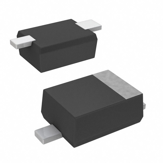
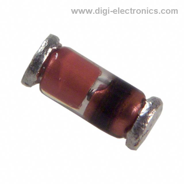
Package details and mounting for the TZMC4V7-GS08 MiniMELF (SOD-80)
The SOD-80 MiniMELF package, utilized by the TZMC4V7-GS08, serves as a refined solution for high-density, precision-oriented circuit assemblies. The cylindrical geometry is engineered to optimize automated surface-mount processes, with lead terminations tailored for consistent engagement during pick-and-place operations. In production environments, the package’s minimal footprint supports close spacing within densely populated PCBs, facilitating significant miniaturization. Its mechanical stability and heat dissipation properties align with the requirements of reflow soldering, minimizing thermal stress-induced defects and ensuring robust joint integrity.
Dimensional tolerances of the SOD-80 package are tightly controlled, supporting reliable electrical isolation between adjacent components even when spacing is reduced to accommodate complex topologies. This is especially evident in critical path designs where signal integrity is paramount. The form factor allows for strategic routing beneath and around the package, providing flexibility in multilayer boards and complex hybrid modules. Attention to package orientation during placement mitigates risk of misalignment and subsequent functional anomalies, an essential consideration in high-throughput surface-mount lines.
Operational advantages are marked in instrumentation circuits and portable electronic devices. Here, size constraints drive aggressive miniaturization, yet demand uncompromising reliability. The SOD-80 MiniMELF consistently meets these dual objectives. Empirical observations confirm its superior resistance to vibration and mechanical shock compared to larger leaded alternatives. Practical deployment has demonstrated stable electrical behavior under repeated thermal cycles, underscoring the package’s suitability for environments subject to temperature fluctuations or high operational duty cycles.
From a design perspective, the package’s geometry simplifies automated optical inspection and test probe access, expediting yield analysis and post-assembly verification. Integration into hybrid modules benefits from the package’s uniformity and well-documented thermal profiles, facilitating predictable performance scaling in multi-component arrays. This seamless merge between mechanical form and electrical function allows for innovative system architectures where conventional packages would pose size or reliability constraints.
A nuanced understanding recognizes that the SOD-80 MiniMELF’s value is magnified in scenarios where layout density, process reliability, and long-term durability intersect. Its deployment within assemblies leveraging the TZMC4V7-GS08 yields quantifiable advantages in throughput, performance stability, and board-level real estate management, positioning the package as a fundamental enabler in next-generation electronic platforms.
Potential equivalent/replacement models for the TZMC4V7-GS08
When selecting functionally equivalent or replacement models for the TZMC4V7-GS08 Zener diode, the analysis begins at the fundamental level of electrical parameters. Core characteristics—Zener voltage, tolerance, maximum power dissipation, leakage current, and thermal stability—represent the electrical signatures that must be matched to ensure system reliability. The TZMC4V7-GS08, anchored at 4.7 V nominal Zener voltage, is frequently matched with alternatives like the TZMB4V7 within the same Vishay TZM-Series, as well as other industry-standard 4.7 V Zener diodes, typically housed in MiniMELF/SOD-80 packages to preserve mechanical interchangeability.
A precise comparison reveals the practical significance of voltage tolerance, with the TZMB variant offering a tighter ±2% clamp versus the ±5% of the TZMC. This distinction is decisive in regulation circuits and voltage references, where margin stacking can compromise precision and long-term drift control. Power dissipation ratings, often standardized within package types but unique across manufacturers, must be verified against worst-case thermal scenarios in the application environment. Neglecting the subtle impact of micro-environment heating and PCB layout on these ratings often manifests as parasitic failures over extended duty cycles.
Application-specific considerations extend beyond the immediate voltage and power parameters. Reverse leakage current, though a minor specification under nominal testing, can become a hidden source of standby power drain in battery-operated and energy-critical systems. Packaging is another non-trivial factor; SOD-80 format ensures compatibility in both automated surface-mount production and repair operations. However, minute differences in lead finish or taping configurations can disrupt automated pick-and-place sequences, stressing the necessity of verifying reel orientation and mechanical fit.
Experience shows that robust designs anticipate variations not just at the level of primary characteristics but in secondary effects. For example, transient thermal impedance and the resulting current surges during ESD events differ subtly between manufacturers, despite stated equivalence. Such factors occasionally reveal themselves only after extensive field deployment or accelerated lifetime testing.
A layered evaluation strategy prioritizes electrical compatibility, validates thermal and mechanical parameters, then iteratively reviews historical field data. Over time, some models build reputations for enduring margin beyond datasheet minimums—a tacit form of engineering knowledge useful when specified tolerances are close to boundary conditions.
In summary, alternate models for the TZMC4V7-GS08 can deliver functional parity when evaluated across voltage, tolerance, dissipation, and mechanical form. However, practices grounded in attention to nuanced parameter differences, alignment with production logistics, and practical application feedback optimize the replacement process and future-proof the design against unforeseen edge cases.
Conclusion
For voltage stabilization circuits where precision and reliability are non-negotiable, the selection of a Zener diode must be rooted in a thorough analysis of electrical and mechanical characteristics. At the foundational level, the Vishay TZMC4V7-GS08 leverages a refined silicon processing method, yielding consistent Zener voltages tightly held to 4.7 V, with minimal deviation across production batches. The device’s low reverse leakage current, even under elevated temperatures, ensures negligible impact on reference voltage integrity, addressing a common challenge in high-density integration environments.
Examining power dissipation capabilities, the TZMC4V7-GS08 exhibits a power rating appropriate for compact, surface-mount configurations, effectively balancing thermal performance and board real estate constraints. Its design permits direct integration onto multilayer PCBs with automated assembly, eliminating concerns about manual placement variability and soldering stress. The diode’s short lead traces and robust construction contribute to stable thermal behavior in scenarios where junction temperature can critically affect voltage regulation accuracy.
In practical deployment, precision analog circuits and digital modules benefit from the TZMC4V7-GS08’s stable breakdown characteristics, especially when subjected to fluctuating supply voltages or sudden transients. Its compatibility with standard SMD footprints facilitates rapid prototyping and seamless transition to volume production, reducing overhead and improving turnaround time across hardware revisions. When component integrity over operational lifecycles is necessary, the device’s proven reliability supports long-term system stability, a core requirement in instrumentation and communication infrastructure.
Strategic utilization of Vishay’s TZM-Series portfolio extends design latitude, allowing circuit architects to select optimal voltage thresholds and package sizes as dictated by signal fidelity requirements, physical layout constraints, and supply chain considerations. This modularity guards against sourcing disruptions, ensuring continuity in manufacturing and maintenance phases. Technical diligence in calculating series resistance, assessing peak pulse energy, and mapping thermal profiles prior to incorporation further refines operational margins, directly elevating overall circuit robustness.
A nuanced understanding of the interplay between leakage, voltage tolerance, and package thermal resistance unlocks incremental improvements in voltage reference stability, especially in low-noise and high-precision feedback loops. The TZMC4V7-GS08’s blend of electrical performance and mechanical versatility naturally aligns with advanced systems such as sensor arrays, portable medical devices, and mobile communications, where both compactness and unwavering voltage regulation are paramount. Subtle optimization of layout topology and thermal relief strategies in these applications will often reveal the hidden reserves of reliability and precision made possible by thoughtful Zener diode selection.