 >
>


Product overview: Vishay VF30200C-E3/4W dual high voltage Schottky rectifier
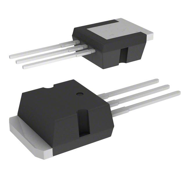
The Vishay VF30200C-E3/4W dual high voltage Schottky rectifier leverages advanced Trench MOS Barrier Schottky (TMBS®) technology to deliver optimized high-speed switching performance and reduced conduction losses. Core to its architecture, the TMBS design minimizes forward voltage drop across a 200 V reverse voltage rating and 15 A continuous forward current capability, ensuring robust efficiency under demanding electrical stress. The common cathode pinout, integrated into a TO-220-3 Full Pack package with an isolated mounting tab, enables straightforward thermal management without additional insulation hardware, addressing one of the critical bottlenecks in compact power electronics assembly.
Analyzing the device from a mechanism perspective, the trench-based Schottky barrier inherently combines the low forward voltage and fast recovery characteristics typical of Schottky diodes, while delivering enhanced avalanche and surge current robustness—a feature especially advantageous in converter topologies prone to inductive overshoots. The common cathode configuration is particularly beneficial for designers targeting center-tapped transformer rectification or freewheeling diode applications in synchronous buck and boost converters. The isolated Full Pack housing further alleviates constraints in board layout where heatsink and electrical isolation must coexist within tight spatial requirements and where traditional metal-backed TO-220s would complicate creepage and clearance.
From the standpoint of system integration, the VF30200C-E3/4W supports increased switching frequencies by minimizing recovery charge and reverse leakage, as compared to planar Schottky or ultrafast silicon rectifiers. This directly translates to downsized magnetic and capacitive components in modern power supply units, yielding both weight and footprint reduction. In custom forward or half-bridge topologies, the rectifier’s dual-channel structure can serve dual independent rails or be parallelized for augmented current capability, contingent on board-level current sharing measures. Notably, integrating schottky rectifiers such as the VF30200C-E3/4W has proven effective in reducing thermal derating margins and extending overall system lifetime under cyclic stress—a critical consideration in automotive and industrial supply domains.
Field deployment underscores the device’s practicality where board real estate is constrained and heat dissipation cannot be sacrificed. The use of a fully encapsulated TO-220-3 allows direct attachment to grounded heatsinks without additional mica or sil-pad insulation, accelerating manufacturing throughput. In experience-backed implementations—such as isolated DC-DC bricks or AC-DC front ends designed for harsh line transients—the device’s surge handling augments overall system immunity, while minimizing power loss even in continuous conduction mode.
Careful device selection within Vishay’s TMBS high voltage family (such as the related V30200C, VB30200C, VI30200C) allows for tailored optimization along the dimensions of conduction loss, switching speed, and package compatibility. This granular control enables power designers to dial in the ideal mix of performance and form factor, rather than compromise toward generic rectification solutions.
Ultimately, the architecture and performance envelope of the VF30200C-E3/4W positions the device as a critical component in contemporary high-efficiency converter and power supply circuits, unlocking superior thermal management, predictable EMI performance, and design flexibility that are fundamental to scaling demanding applications. In practice, its deployment simplifies compliance with elevated regulatory and reliability standards while facilitating faster transition to production-ready designs.
Core features and benefits of VF30200C-E3/4W series
The VF30200C-E3/4W series leverages advanced Trench MOS Schottky fabrication to achieve a low forward voltage drop, precisely 0.526 V at a 5 A forward current. This inherently reduces conduction losses, making these devices highly suitable for power architectures where efficiency targets are stringent, such as DC-DC converters and synchronous rectification stages. The underlying device structure—combining a finely controlled trench geometry with high-purity Schottky barriers—minimizes reverse recovery losses, thus curtailing thermal buildup and facilitating consistent performance during extended high-load cycles.
Thermal management is optimized through low junction-to-case thermal resistance, improving heat dissipation and permitting simplified cooling strategies. In practical terms, the device withstands repeated high-temperature soldering processes—rated at 275 °C for 10 seconds as specified by JESD 22-B106—without degradation in electrical performance or mechanical integrity. This resilience directly supports high-volume automated assembly lines where throughput and yield are tightly coupled to process reliability. Attention to package material selection and lead finish not only assures robust solderability but also mitigates potential oxidation or interface issues during multiple reflow passes.
RoHS compliance and MSL Level 1 grading allow seamless integration into forward-looking product designs, addressing both legislative mandates and supply chain reliability standards. The encapsulation employs UL 94 V-0 molding compounds, enhancing flammability resistance—a critical factor in dense or safety-critical assemblies. This choice of materials and finish ensures minimal risk of process-induced latent defects and long-term field reliability.
When deployed in switch-mode power supplies, battery chargers, or solar micro-inverters, the VF30200C-E3/4W series demonstrates stable efficiency profiles and predictable thermal behavior, even in parallel or dissipative operating modes. Direct experience highlights the reduction in component count enabled by its low loss characteristics; systems benefit from lower heatsink requirements and reduced derating, streamlining both the BOM and the physical architecture.
A subtle benefit emerges from the synergy between low forward voltage and stable thermal character: designers can push operating frequencies or compact layouts without incurring penalty in device lifetime or system robustness. This flexibility drives competitive differentiation in both consumer and industrial sectors, where footprint, responsiveness, and lifetime cost are pivotal.
Integrating Trench MOS Schottky devices such as VF30200C-E3/4W thus enables higher system-level efficiencies while maintaining manufacturability and compliance, supporting scalable adoption across evolving power conversion technologies.
Electrical specifications and performance characteristics of VF30200C-E3/4W series
In-depth analysis of the VF30200C-E3/4W series dual Schottky rectifier reveals how specific electrical characteristics shape device selection and circuit performance. The 200 V repetitive peak reverse voltage indicates suitability for applications demanding moderate voltage standoff, such as secondary-side rectification in high-frequency switch-mode power supplies. The 15 A total forward current capacity accommodates substantial continuous loads, ensuring robust operation under elevated currents commonly encountered in power converters.
Schottky diode architecture in this series delivers inherently low forward voltage drop, significantly reducing conduction losses during rectification. This property, coupled with minimized reverse leakage, enhances overall efficiency—especially in contexts where thermal management is a concern. When evaluating transient and steady-state thermal requirements, forward derating curves become pivotal, providing granular insight into permissible current as a function of temperature. This enables targeted heatsinking and layout strategies, directly influencing board-level reliability under cyclical loading.
Switching performance analysis benefits from instantaneous current-voltage profiles, which reveal the device’s response during rapid transitions. Fast switching capability minimizes energy lost to reverse recovery, a recurring bottleneck in conventional silicon rectifiers. Engineering evaluation often centers on these parameters when targeting converters operating at frequencies upward of the hundreds of kilohertz; the VF30200C-E3/4W series sustains efficient operation with minimal overshoot or ringing—a critical factor in maintaining signal integrity and suppressing electromagnetic interference.
Power loss curves offer a comprehensive mapping between operational points and thermal output, supporting precise allocation in overall system energy budgets. For high-density designs aiming for reduced form factor and elevated power throughput, aligning device selection with these curves improves temperature stability and allows successful implementation of compact cooling strategies. Practical experience shows clear performance retention in custom layouts leveraging low-resistance PCB traces and forced-air convection, especially where ambient temperature excursions cannot be fully controlled.
Transient thermal impedance characteristics provide valuable insight for fault tolerance and protective scheme design. Rapid thermal excursions during switching surges or overload conditions require devices with predictable and fast heat propagation behavior; advanced simulation based on manufacturer-supplied profiles streamlines placement of thermal sensors and fusing elements, resulting in greater system uptime and reduced field failures.
Junction capacitance parameters profoundly affect noise generation and waveform fidelity, particularly in high-speed or low-voltage signal applications. Low junction capacitance mitigates charge accumulation across frequency shifts, facilitating clean output and improved efficiency in synchronous rectification schemes. Integrated into RF power applications, this leads to measurable reductions in cross-talk and parasitic oscillations. Leveraging the VF30200C-E3/4W series’ refined electrical profile supports design of tightly coupled, high-frequency modules with sustained reliability.
Careful correlation between datasheet metrics and real-world circuit demands ensures that implementation achieves both efficiency and longevity. Selecting devices with tailored forward and reverse profiles yields enhanced switching performance under dynamic loads, while maintaining energy loss and thermal stress within prescribed margins. Based on field observation, the optimal balance of electrical and thermal management provided by the VF30200C-E3/4W series offers a distinct advantage for power conversion schemes requiring robust, low-loss operation in compact layouts.
Mechanical construction and package options for VF30200C-E3/4W series
Mechanical integration of the VF30200C-E3/4W series hinges on the robust selection of package types optimized for diverse assembly environments. The device’s primary enclosure, the TO-220AB ITO-220AB configuration with an isolated tab, exhibits a critical advantage: direct compatibility with conventional through-hole PCBs and industry-standard heatsink attachments. This isolated tab architecture enhances electrical isolation while simplifying system-level insulation requirements, streamlining module-level safety certification and reducing additional materials.
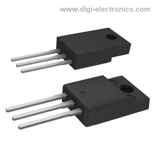
Expanding beyond the baseline, the series incorporates supplementary options such as TO-262AA and D²PAK (TO-263AB), which address alternate mounting methods, especially where automated surface-mount assembly or compact layout is prioritized. The low-profile D²PAK, for instance, offers improved thermal performance in high-density power architectures by shortening the thermal path to dedicated PCB copper planes. Within practical design scenarios, package selection frequently balances cooling strategy, board real estate constraints, and assembly process costs; the presence of leaded and leadless options across the VF30200C series directly supports such decision making, accelerating time-to-market for power stage designers navigating cross-platform requirements.
Engineering attention to surface quality is manifest in the matte tin terminal finish, which not only supports robust solder joint formation but also counters whisker growth—an acute failure mode in power electronics—through compliance with contemporary international standards. This aligns to reliability roadmaps in demanding automotive, industrial, or commercial systems, lowering the risk of latent shorts and simplifying long-term maintenance calculations. When developing thermal management paths, the manufacturer’s provided dimensional data and recommended pad layouts act as a foundation for subsequent simulation and empirical characterization. Utilizing such application documentation enables rapid prototyping and iterative verification of joint strength, pad fill, and cooling efficiency, especially when aligning with specific derating protocols.
A distinguishing strategy is the series’ focus on packaging modularity within a single electrical family. This modularity establishes a coherent qualification pipeline—designers can scale a verified design across different platforms or thermal benchmarks merely by substituting the package type, without full requalification of the die or layout, thus preserving validation effort. The combination of isolation, finish quality, package diversity, and well-documented mechanical interfaces forms a toolkit for designers to resolve both initial integration and field-level durability issues in a systematic, standards-aligned fashion, fostering resilient high-power switching solutions even in variable application settings.
Typical application scenarios for VF30200C-E3/4W series
The VF30200C-E3/4W series leverages its synergistic combination of high voltage tolerance, substantial forward current ratings, and ultra-low loss characteristics to address stringent requirements across multiple high-reliability power electronic ecosystems. At the device physics level, the series exhibits minimal reverse recovery charge and a soft recovery profile, directly translating to suppressed EMI generation and improved switching efficiency within high-frequency topologies. These attributes prove essential in switch mode power supplies (SMPS), where sub-microsecond recovery time enables optimized drive cycles and tighter thermal budgets. Such performance allows designers to push switching frequencies above conventional limits without suffering conduction or switching loss penalties, thereby shrinking passives and magnetic footprints for advanced miniaturization.
Freewheeling and reverse polarity protection in DC/DC converter systems benefit from the VF30200C-E3/4W’s low forward voltage drop and robust avalanche capability. When deployed as a secondary-side synchronous rectifier or as a series protection element, the device maintains negligible energy loss during conduction and minimizes power dissipation even under extended transient conditions. This fortifies system reliability in distributed bus architectures, particularly where load step dynamics or input inrush profiles present a risk to semiconductor integrity. Experience shows that the device excels in harsh supply rails frequently subjected to brownout and hot-plug events, preserving both system uptime and critical signal margins.
In OR-ing applications, especially for parallel power modules targeting high-availability outcomes, the VF30200C-E3/4W’s rapid turn-on/turn-off times and matched leakage behavior suppress unwanted cross-currents. This translates into deterministic module sequencing and prevents failover-induced backfeeding, elevating the resilience of telecom rectifiers and redundant supply backbones. The package’s engineered low thermal impedance facilitates direct interface with compact heatsinks or multilayer copper planes, streamlining thermal path management in spatially constrained racks and densely integrated enclosures. This capability reduces the necessity for complex thermal interface designs, permitting straightforward adoption even in high-altitude or elevated ambient deployments.
Automotive and industrial platforms, where extended temperature operation and long-term cycling are baseline requirements, particularly value the VF30200C-E3/4W series’ robust junction construction and stable forward characteristics across temperature gradients. Field data demonstrates lower failure rates and improved lifetime cost metrics, contributing to global quality and compliance benchmarks. Notably, the device’s consistent parametric performance over extended mission profiles directly supports predictive maintenance strategies and helps ensure regulatory readiness in electromobility and critical infrastructure domains.
The VF30200C-E3/4W’s capabilities do not merely suit existing frameworks; they actively encourage system architectures that pair efficiency with resiliency. By reducing design margins previously allocated to loss, recovery, and thermal uncertainty, engineering teams gain the latitude to innovate at the level of both topology selection and layout integration. This series ultimately supports a paradigm shift toward highly efficient, compact, and inherently reliable power conversion solutions suitable for next-generation electronic platforms.
Potential equivalent/replacement models for VF30200C-E3/4W series
Selecting equivalent or alternative models for the VF30200C-E3/4W series involves multilayered evaluation along core technical vectors. The VF30200C-E3/4W, part of Vishay’s TMBS® (Trench MOS Barrier Schottky) portfolio, exhibits defined electrical profiles: dual-common cathode Schottky rectification, 200V reverse voltage, and 30A forward current handling. Key sister variants—such as V30200C, VB30200C, and VI30200C—share the electrical die but differ in package outlines, termination style, or screening level. Package distinctions hold critical importance in both reflow and through-hole assembly lines, as form factor affects not only PCB footprint compatibility but also thermal conduction and assembly yield. Employing second sources within the TMBS® family minimizes validation inertia given guaranteed parametric congruity, yet documenting subtle differences in lead finish, creepage distances, and junction-to-case resistance can prevent downstream integration surprises, especially when moving between TO-247, TO-220AB, and ITO-220AB profiles.
Beyond the internal family, cross-referencing to analogous dual Schottky models from peer manufacturers—such as ON Semiconductor’s MBRS30200CT or STMicroelectronics’ STPS30200CT—requires disciplined verification of voltage margin, surge tolerance, and forward voltage drop under realistic operating pulses. Discrepancies in reverse recovery times become more pronounced in high-switching or synchronous rectification circuits, where device selection can influence EMI behavior and system-level power losses. Cross-manufacturer thermal impedance (RθJC) variances often surface during sustained high-load operation, and engineering practice confirms that explicit review of datasheet graphs—typical forward drop vs. current, derating curves at elevated case temperatures—offers substantial predictive value.
Deploying alternative models also demands scrutiny of mechanical robustness, particularly solderability under lead-free conditions and package stress survivability during board-level reliability tests. Experiences in demanding power supply layouts highlight that minor differences in package molding compound or lead frame design can affect automated optical inspection and even thermal cycling-induced fatigue. Furthermore, subtle shifts in pinout convention or marking orientation between vendors could trigger test or assembly firmware revision, underlining the non-obvious layers to effective cross-qualification.
In application, aligning substitute devices with VF30200C-E3/4W’s feature set is fundamental for power rectification in SMPS secondary stages, freewheeling diodes in bridge configurations, or output sections in high-current chargers. Real-world design cycles benefit from maintaining a qualification matrix recording both electrical and thermomechanical findings—this enables proactive risk mitigation during procurement fluctuations. A core insight emerges: Validating not only datasheet specifications but also operational margins and corner-case thermal limits delivers robust system performance, particularly as power density and certification standards tighten. Through methodical comparison and layered analysis, engineering teams foster supply chain agility without compromising circuit reliability.
Conclusion
The VF30200C-E3/4W series dual high-voltage Schottky rectifiers leverages advanced barrier technology to minimize forward voltage drop while maintaining low reverse leakage, directly addressing the efficiency bottlenecks prevalent in high-frequency, high-power designs. Core to its performance is the integration of state-of-the-art Schottky diodes capable of operating under sustained forward currents up to 30A and reverse voltage ratings reaching 200V. The rectifier’s characteristic fast switching behavior, derived from the absence of minority carrier storage, sharply reduces recovery losses—an essential attribute in resonant and synchronous topologies where switching frequency and transient response are critical performance metrics.
Mechanical design flexibility is ensured through its robust TO-247AD package, facilitating simplified thermal interface engineering and reliable mounting in densely populated layouts. The substantial creepage and clearance distances in the package design support safer operation in high-voltage assemblies, and the hermetic sealing techniques offer resilience during reflow and wave soldering cycles—minimizing the risk of moisture or contaminant ingress that could compromise long-term reliability.
When aligning the VF30200C-E3/4W with application-specific requirements, several parameters demand careful scrutiny. Forward voltage (V_F), peak repetitive reverse voltage (V_RRM), and maximum junction temperature delineate the operational envelope. The substantial surge current capability allows for robust absorption of load transients, making the device adaptable to diverse topologies such as full-bridge, center-tap, or freewheeling configurations in switched-mode power supplies (SMPS), power factor correction (PFC) stages, and motor drive inverters. Experience indicates that derating the device for elevated ambient temperatures and ensuring sufficient heatsinking further enhances operational margins, particularly in tightly regulated and thermally dynamic environments.
From a manufacturing integration standpoint, the Schottky’s lead-free, RoHS-compliant design streamlines qualification for eco-conscious and geographically regulated sectors. The inclusion of high-reliability assurance via rigorous production-level stress testing underpins long field lifespans, limiting early failure rates in mission-critical deployment scenarios. In comparing alternatives, engineers benefit from benchmarking reverse recovery time and avalanche energy ratings, where the VF30200C-E3/4W maintains competitive advantage through minimized switching losses and enhanced ruggedness against voltage transients.
A unique aspect for circuit designers is the device’s balanced compromise between high-frequency agility and bulk power management without sacrificing either efficiency or durability. Intuitive selection rooted in precise matching of device specifications to operational regime, coupled with attention to layout and cooling details, crystallizes the VF30200C-E3/4W as a preferred solution in next-generation power conversion architectures. This explicit harmonization of electrical, mechanical, and reliability parameters enables maximized system-level performance when transitioning from design to mass production.