>
>


Product overview of Vishay BYG20J-E3/TR
The Vishay BYG20J-E3/TR rectifier exemplifies strategic engineering for high-frequency, high-voltage environments where fast switching and reliability are paramount. Anchored by an avalanche capability, its silicon junction suppresses transient voltage surges, avoiding breakdown phenomena that often compromise device integrity. This mechanism, combined with an ultrafast recovery structure, enables efficient performance in circuits susceptible to voltage spikes or switching noise, such as snubber networks and secondary-side rectification in offline switch-mode power supplies.
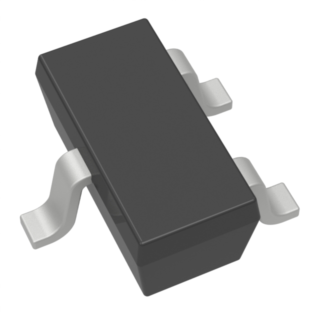
Within the surface-mount DO-214AC (SMA) package, the BYG20J-E3/TR achieves thermal management, mechanical robustness, and minimal PCB footprint. The form factor facilitates automated assembly and dense layouts, aligning with evolving design trends in power conversion modules and compact consumer equipment. Its 600 V repetitive peak reverse voltage extends compatibility to applications like flyback converters, LED drivers, and motor control inverters, where voltage spikes are routine and operating endurance is crucial.
Current conduction up to 1.5 A continuous—paired with ultrafast recovery time—minimizes reverse current losses and electromagnetic interference. This design approach supports high-efficiency standards, enabling compliance within regulatory constraints on standby power and harmonic emissions. Engineers leveraging similar Vishay devices, including BYG20D and BYG20G, will recognize a shared platform but may note that BYG20J’s elevated voltage rating and avalanche characteristics distinctly position it for more stringent applications, such as industrial automation loops and telecom line interfaces.
Real-world deployment shows consistent junction reliability under pulse stress, with careful attention to PCB thermal design further optimizing performance. Integrating the BYG20J-E3/TR in synchronous rectifier circuits or fast recovery diode arrays illustrates its capability to handle high di/dt events without excessive switching losses or degradation. Bench evaluations highlight the device’s capacity to retain recovery integrity under both regulated and poorly filtered loads, a decisive factor when balancing circuit compactness against long-term reliability.
A subtle yet critical insight emerges when selecting components for next-generation lightweight systems: avalanche-rated rectifiers like the BYG20J-E3/TR not only absorb unexpected electrical transients but also streamline protection strategies, reducing the need for parallel suppression elements. This inherently boosts system reliability, lowers costs, and simplifies qualification cycles—an outcome that discerning system architects can exploit for differentiated product platforms.
Key features and technical advantages of Vishay BYG20J-E3/TR
The BYG20J-E3/TR epitomizes a targeted approach to optimizing power semiconductor functionality, integrating several design elements that respond directly to industry demands for efficiency and reliability. At the foundational level, the incorporation of a glass-passivated pellet chip junction underpins the device’s electrical stability; such passivation techniques mitigate micro-leakage and guard against junction degradation, ensuring consistent form factor and long-term operational integrity under thermally stressful conditions. This architectural choice results in predictable forward voltage characteristics, crucial for maintaining system balance in high-density layouts.
A defining trait of the BYG20J-E3/TR is its ultrafast reverse recovery time—a parameter engineered to minimize switching losses in rapid current commutation scenarios typical of SMPS (switched-mode power supply), motor controls, and inverter topologies. By reducing the interval required for the diode to block reverse current after forward conduction, designers can extract higher switching frequencies and boost overall efficiency, directly impacting both power throughput and thermal management. This aspect not only lowers cooling demands but also contributes to extending component life due to reduced transient-induced stress.
Low reverse current specification is another pivotal engineering feature. Leakage currents manifest as silent power drains and may precipitate instability, especially in precision analog and control circuits. By suppressing leakage to minimal levels, the BYG20J-E3/TR supports stringent noise budgets and maximizes energy conservation, making it particularly suited to energy-sensitive platforms ranging from IoT micro-power modules to instrumentation interfaces.
Soft recovery dynamics—embedded within the silicon structure—address voltage transients inherent in snappy switching events. The suppression of peak reverse voltage changes protects adjacent sensitive elements and lessens EMI propagation pathways. In multi-stage converters or automotive ECUs, where switch-induced spikes can compromise system logic, the presence of controlled recovery softness elevates overall system robustness and simplifies EMI management schemes, reducing the need for extensive external filtering.
The surface-mount package design brings a clear production advantage, allowing direct integration into automated SMT production lines. Dimensional and process compatibility with standard placement and reflow technologies lowers total assembly cost and enhances throughput, while ensuring repeatable solder joint quality. This packaging agility responds well to high-volume manufacturing pressure, streamlining logistics and quality assurance processes.
Environmental and regulatory compliance is embedded at the product’s core. RoHS adherence and halogen-free options align with global directives, easing cross-market deployment and supporting eco-centric procurement strategies. Automotive-grade quality is facilitated through optional AEC-Q101 qualification, ensuring resilience against grades of mechanical and thermal stress encountered in vehicular or industrial installations.
In practical deployment, the device’s characteristic profile supports circuit architectures where thermal headroom is limited and operational cycles are intense. For instance, in compact inverter assemblies where board space is at a premium, leveraging the BYG20J-E3/TR’s minimal leakage and stable recovery pattern can obviate the need for additional snubber or buffer components, streamlining the BOM and facilitating maintenance cycles. Engineering choices such as robust passivation and targeted recovery tailoring demonstrate a nuanced understanding of end-system requirements, delivering not only high immediate performance but also predictable service reliability across diverse operational timelines.
Mechanical characteristics and reliability assurances of Vishay BYG20J-E3/TR
Mechanical performance and reliability of the Vishay BYG20J-E3/TR are governed by a synthesis of material selections, structural standards, and targeted test regimes. The DO-214AC (SMA) package delivers a robust, compact footprint designed to optimize board space utilization for dense PCB layouts while minimizing mechanical stress under vibration and thermal cycling. Its adherence to UL 94 V-0 ensures self-extinguishing behavior in high-temperature projects, directly supporting system-level safety in applications prone to electrical overstress or short-circuit fault conditions.
Leads feature a solderable matte tin finish, applied to align with J-STD-002 and JESD 22-B102 protocols, thus demonstrating extensive compatibility with automated reflow and wave solder processes. This compatibility not only simplifies surface-mount integration but also addresses issues such as wetting consistency and the suppression of tin-lead intermetallic growth, which are critical for long-term connection integrity, especially under temperature fluctuations and repeated thermal exposure common in power supply and industrial control assemblies.
Mechanical reliability extends to the whisker mitigation strategies of the E3, M3, HE3, and HM3 suffix codes—each manufactured to meet JESD 201 class 2 criteria. These specifications form a barrier against microstructural failures associated with tin whisker growth, which otherwise risk short circuits in high-density modules, particularly where equipment uptime is paramount. This intrinsic level of conformity underlines the component’s viability in harsh environments characterized by mechanical shock and shifting loads, often observed in transportation and energy sectors.
Clear cathode color banding expedites visual inspection, streamlining error-proofing steps during high-volume or automated assembly. Such simple yet decisive markings are frequently overlooked, but experience reveals their significant impact in post-solder verification and field service scenarios, where rapid, accurate identification reduces rework and downtime.
Automotive-qualified variants are tested beyond the base industrial specification, conforming to AEC-Q101 standards that examine parametric stability under extended thermal, electrical, and intermittent load extremes. Qualification extends confidence to mission-critical applications—engine controls, ADAS modules, or inverters—where regulatory compliance and operational longevity intersect.
Experience with this series confirms that the collective design and test pedigree of the BYG20J-E3/TR not only lowers lifetime maintenance burdens but also streamlines inventory management through universal footprints and consistent lot quality. In demanding applications, integrating such parts early during design offers downstream insurance against systemic mechanical failures, underlining the foresight of selecting components subjected to robust, multi-domain verification processes. The device’s track record in cross-sector deployments highlights its role as a foundation for dependable, scalable electronic systems.
Typical applications for Vishay BYG20J-E3/TR
The BYG20J-E3/TR diode is engineered for scenarios that require efficient high-frequency rectification, where both low reverse recovery time and rugged avalanche energy handling are critical. At the device level, its fast-switching characteristics directly reduce losses in synchronous rectification stages, maximizing efficiency in power topologies such as flyback and forward converters. Its robust avalanche ratings allow design architectures to tolerate voltage spikes and transient overload conditions without compromising overall reliability.
Within switching power supplies and DC-DC converters, the BYG20J-E3/TR serves not only as a main or output rectifier, but also as a snubber or clamp diode to suppress switching node oscillations. This ensures increased noise immunity and less stress on control circuitry. In inverter designs, particularly those used for motor control or uninterruptible power systems, its rapid recovery features ensure minimal dead-time and lower EMI emissions—addressing both regulatory and operational constraints in dense electronics environments.
In the context of consumer electronics, deployment as a freewheeling diode ensures swift handling of inductive load energy during switch-off events, thereby mitigating voltage surges that could otherwise damage power semiconductors. The diode’s low-leakage characteristics contribute to reduced standby losses in battery-operated or energy-conscious endpoints, which is particularly beneficial where energy regulations are stringent. The integration of these parameters facilitates aggressive PCB layout strategies and high-switching frequency designs without the penalty of thermal hotspots or reduced component lifetime.
For automotive platforms, the availability of AEC-Q101 qualified variants positions the BYG20J-E3/TR as a suitable solution for harsh operating domains. The ability to provide stable performance across wide junction temperature swings, coupled with resistance to mechanical shock and vibration, allows confidence in ECUs, lighting modules, and power distribution applications. Its proven immunity to electrical transients, such as those defined by ISO load dump and EFT standards, aids in minimizing failure rates during field operation.
Telecommunication infrastructure benefits from the diode’s consistent low-leakage profile and tight recovery time distribution, enabling reliable operation in base stations, routers, and optical network units. These features are essential where circuit redundancy and long operating lifespans are fundamental requirements. Design experience underscores the advantage of integrating devices like the BYG20J-E3/TR in parallel diode arrays for distributed rectification, balancing current sharing and mitigating localized heating effects—a consideration in modular and rack-based deployments.
Optimal application of the BYG20J-E3/TR involves early attention to both thermal management and circuit parasitic parameters. These considerations, in combination with the device’s fundamental strengths, yield solutions that meet stringent reliability targets, particularly in miniaturized, high-density designs pushing the envelope of switching speed and robustness.
Ratings, electrical characteristics, and performance curves of Vishay BYG20J-E3/TR
The Vishay BYG20J-E3/TR is a fast-recovery rectifier designed with robust electrical ratings tailored for medium-power switching and rectification. At a nominal 25 °C ambient environment, it maintains a continuous forward conduction capacity of 1.5 A, while withstanding repetitive reverse voltages up to 600 V. These ratings are anchored in its planar junction construction, which balances low forward voltage drop with elevated blocking capability—an essential attribute for rectifiers deployed across diverse power conversion stages.
Delving into forward characteristics, the forward voltage drop versus current profile, typically peaking near 1.0 V at the rated forward current, emerges from the device’s low series resistance and controlled doping gradients. This ensures efficient conduction, minimizing thermal buildup during sustained operation. Such behavior can be directly traced to its semiconductor geometry—wider base regions offer lower losses but necessitate precise doping control to avoid excess reverse leakage. In practical design, this translates to lower heatsink requirements, especially when configuring multiple devices in parallel for load sharing.
Reverse characteristics present another layer of critical performance. Reverse leakage current, charted as a function of junction temperature, remains minimal under recommended operating limits, supporting long-term reliability in high-temperature settings. However, as junction temperature rises—owing to either high ambient environments or system power cycles—reverse leakage increases exponentially, dictated by intrinsic carrier generation. Deploying the BYG20J-E3/TR in high-density boards thus necessitates attention not only to initial layout, but also to dynamic airflow and substrate thermal coupling, in order to keep cumulative leakage and resultant power dissipation in check.
The reverse recovery profile is a focal point for high-frequency designers. The recovery time, typically measured in tens of nanoseconds, reflects the engineered minority carrier lifetime and junction topography. This characteristic dictates the rectifier’s suitability in fast-switching topologies, such as continuous-mode flybacks or phase-shifted full-bridge inverters, where excessive recovery charge manifests as switching loss and noise. Engineers can reference the provided recovery charge and time curves to select optimal snubbing networks or gate-drive dead times, fine-tuning the commutation waveform to minimize EMI generation.
Thermal and frequency performance represent intersecting layers of device behavior. Reverse power dissipation as a function of junction temperature, detailed in the device's power curves, underlines the need for robust heat sinking and realistic thermal modeling at the system level. Unlike diodes with significant junction capacitance, the BYG20J-E3/TR maintains a moderate junction capacitance profile, as indicated by capacitance-voltage curves. This enables stable, predictable performance even in resonant tank applications or active-clamp configurations, where capacitive reactance could otherwise introduce signal distortion or oscillation.
Application integration further leverages these core behaviors. In boost PFC stages or unconventionally modulated SMPS outputs, the device’s swift recovery and tight leakage attributes reduce overall energy penalty associated with switching transitions. Experience shows that incorporating the BYG20J-E3/TR in output rectification, particularly where efficiency is strictly monitored, results in both lower thermal stress on magnetic components and fewer downstream filtering requirements. Its performance envelope thus serves not only traditional rectification, but also auxiliary snubber/clamper circuits tasked with transient protection in environments prone to surge or ringdown.
The BYG20J-E3/TR exemplifies an engineering-driven tradeoff—balancing speed, voltage headroom, and allowable leakage with minimal forward drop. This repertoire, informed by device-level silicon optimization, positions it well for use in demanding, space-constrained topologies, where system-level efficiency and component longevity are primary metrics.
Package dimensions and mounting guidelines for Vishay BYG20J-E3/TR
The Vishay BYG20J-E3/TR utilizes the DO-214AC (SMA) surface-mount package, engineered to meet stringent space and thermal constraints prevalent in high-density PCB assemblies. This standardized outline, with typical dimensions of 4.6 mm × 2.8 mm, ensures compatibility with automated pick-and-place processes and supports consistent soldering profiles across mass production. Within engineering workflows, precise adherence to the mechanical envelope not only supports assembly line throughput, but also mitigates risks of package overstress or insufficient clearances that could induce latent reliability issues.
Critical to electrical and thermal reliability is the recommended mounting pad geometry. Vishay’s guidelines stipulate pad dimensions and solder mask openings designed to balance solder joint volume, heat dissipation paths, and manufacturability. Notably, an optimized pad layout minimizes thermal resistance from the junction to ambient, which is especially significant in power rectification or surge protection roles where the device may encounter high peak currents. In addition, the carefully defined pad spacing reduces parasitic inductance and capacitance, thus preserving switching performance at high frequencies—a factor often overlooked in discrete component integration on multilayer substrates.
Choice of substrate material further influences thermal cycling endurance and mechanical robustness. Epoxy-glass (FR-4) offers a well-understood thermal expansion profile and cost efficiency, while Al-oxide ceramics provide superior thermal conductivity and electrical insulation for applications demanding higher power density or enhanced heat sinking. Manufacturing observations indicate that matching CTE (coefficient of thermal expansion) between the package and PCB substrate is paramount to preserving solder integrity through repeated temperature excursions, preventing micro-cracking or voids that degrade long-term device performance.
The DO-214AC footprint’s standardized form factor supports streamlined CAD library management for schematic and layout teams, reducing design validation effort in layouts requiring BOM flexibility or late-stage swaps. Integration with multi-layer PCBs is facilitated via carefully managed solder mask clearance to prevent solder bridging, enabling higher layer counts without compromising assembly yield.
From a systems viewpoint, respecting these mechanical and mounting recommendations eliminates a class of failure modes often manifesting only during field operation. Empirical testing validates that optimized mounting pads, in conjunction with qualified reflow profiles, yield joints exhibiting consistent pull strengths and high resistance to thermal fatigue. In quick-turn designs, consulting empirical solder joint inspection data alongside reference layouts accelerates first-pass yield and expedites overall project timelines.
An underlying insight is the significant leverage package discipline exerts on system-level reliability—not merely at the device, but in ensuring signal integrity, predictable thermal budgets, and streamlined volume manufacturing. Integrating this knowledge early in design phases ensures the BYG20J-E3/TR performs robustly within the broader product architecture, substantiating both electrical and operational metrics over the lifecycle of the assembly.
Potential equivalent/replacement models for Vishay BYG20J-E3/TR
Identifying direct equivalents or suitable replacements for the Vishay BYG20J-E3/TR requires careful analysis of electrical parameters, package compatibility, and required certifications. The BYG20J-E3/TR serves as a fast-recovery rectifier diode with a 600 V reverse voltage rating in a compact DO-214AC (SMA) package, making it a standard choice in power supply circuits, snubber networks, and input protection stages. When a full 600 V rating is not critical, the BYG20D and BYG20G variants present themselves as practical alternatives, featuring similar mechanical footprints and manufacturing quality, but with 200 V and 400 V reverse voltage ratings, respectively. This alignment means that for replacement scenarios, the voltage headroom should always be reassessed with respect to the circuit’s peak reverse voltage during operation and fault conditions; substituting with a lower-rated device, while cost-attractive, introduces the risk of premature field failures if transients exceed device limits.
Vishay’s product range supports streamlined procurement by providing both standard and automotive-qualified rectifiers. Automotive-grade requirements are addressed with the HE3 or HM3 suffixes, indicating compliance with the AEC-Q101 standard for enhanced reliability under high-temperature and vibration stress. The suffix system aids in simplifying bill-of-materials management for designs targeting automotive or industrial platforms, where regulatory compliance is mandatory and long-term supply assurance is critical. Diligent cross-verification between datasheets uncovers subtle variations in parameters such as forward surge current capability, recovery time, and junction temperature ratings, all of which have direct implications on thermal budgeting and electromagnetic interference characteristics. Application-driven selection, such as fast switching in high-frequency SMPS topologies, can make reverse recovery time a differentiating factor—even within similar model families.
A recurring challenge in equipment maintenance and legacy system upgrades is ensuring physical and electrical compatibility in densely packed PCBs. Vishay’s adherence to standardized SMA footprints streamlines direct device swaps. However, in real-world sustainment projects, attention must also be paid to solderability finish and trace layout, particularly when different suffixes or revision codes are introduced. The engineering recommendation is to validate form, fit, and function at both schematic and PCB layout stages and consider small-batch pilot testing whenever introducing an alternative model, especially when operating near the upper threshold of device ratings.
One nuanced consideration is the trade-off between over-specification for universal deployment and cost optimization for specific design margins. For circuits with significant voltage derating practices, adopting the highest voltage option such as BYG20J-E3/TR simplifies inventory but may carry unnecessary cost or introduce slightly inferior performance in terms of forward drop. Conversely, matching device ratings more closely with application needs increases inventory complexity but optimizes BOM cost and potentially thermal efficiency. The key is disciplined voltage qualification during the design phase and rigorous qualification testing for every replacement path.
Overall, the process of identifying and validating substitutes like BYG20D or BYG20G within the Vishay portfolio centers on precise alignment of voltage, current, reliability, and compliance demands. Using structured datasheet review and in-circuit validation, engineers mitigate replacement risks and maintain long-term reliability, while nuanced model selection enables cost-effective, technically robust system design and maintenance.
Conclusion
The Vishay BYG20J-E3/TR ultrafast avalanche SMD rectifier integrates a set of advanced mechanisms that address key power management challenges in contemporary electronic designs. At the semiconductor level, its avalanche capability allows for controlled handling of voltage spikes, significantly reducing susceptibility to transient-induced breakdown. The ultrafast recovery attribute stems from optimized junction engineering and low minority carrier lifetime, resulting in minimized switching losses and efficient performance in high-frequency rectification scenarios. This device consistently demonstrates negligible leakage current, even after extensive thermal cycling, reflecting its robust construction and careful material selection. The SMA package configuration further simplifies PCB integration, offering stable solderability and mechanical resilience required for automated assembly lines.
Exploring real-world application, the BYG20J-E3/TR proves essential in switch-mode power supplies (SMPS), DC-DC converters, and protection circuits—where rapid recovery and high surge tolerance directly translate into improved power efficiency and decreased electromagnetic interference. Automotive architectures, for example, demand devices capable of enduring load-dump events; here, the rectifier’s avalanche rating and high junction temperature operation safeguard critical subsystems under unpredictable power conditions. Telecommunications hardware benefits from the device’s extended qualification range, ensuring continued reliability amidst voltage fluctuations and accelerated thermal aging. In consumer electronics, minimized leakage and quick switching contribute to meeting strict standby power requirements without compromising device longevity.
Comparative evaluation with alternative rectifiers underscores the relevance of subtle specification differences: selecting equivalents such as the 1N5822 or SBYV27 must factor forward voltage drop, recovery time, and mechanical compatibility. Standardization to SMA packages streamlines rework and volume procurement, yet minute disparities in surge ratings or qualification protocols can have significant implications on field failure rates over extended deployment. Leveraging cross-reference databases and parametric search tools not only expedites component selection but also supports cost optimization without sacrificing system integrity.
A nuanced understanding of these technical vectors directly enhances product design, ensuring longevity and stable in-field operation. Careful attention to the interplay between device characteristics and the end-use architecture results in lower warranty claims and higher user satisfaction, validating the decisive role of the BYG20J-E3/TR in mission-critical assemblies. Examining long-term deployment data consistently affirms the strategic value of qualified avalanche rectifiers, especially in electrically demanding topologies where conventional recovery diodes underperform. The integrative approach to selection—considering both electrical and mechanical metrics—drives competitive differentiation and robust performance across industry verticals.