>
>


Product Overview: SI5315B-C-GM Clock Multiplier
The SI5315B-C-GM represents a specialized architecture for clock multiplication and jitter attenuation, calibrated for the stringent timing requirements of networking infrastructure. The device’s internal fractional-N PLL topology underpins its ability to translate and regenerate clock signals across a wide spectrum, seamlessly supporting input and output frequencies from 8 kHz to 125 MHz. This clock signal agility enables interoperability between diverse protocol domains, such as synchronous optical networking equipment and packet-based Ethernet links, where timing tolerances differ markedly.
Layered performance analysis reveals the IC’s low-jitter characteristics, achieved through proprietary loop filter design and optimized noise shaping. The sub-ps RMS phase jitter metrics directly translate to enhanced bit error rates within high-speed serial interfaces, mitigating the risk of data corruption caused by clock instability—particularly evident in densely populated switch fabrics. Embedded clock distribution drivers further allow scalable clock fanout while preserving edge integrity, which is essential as timing signals traverse different PCB domains and cable segments.
Deployments in line card and switch architectures consistently demonstrate the SI5315B-C-GM’s resilience to input frequency distortion and supply rail noise. Systems engineers typically observe cleaner eye diagrams and increased margin against timing violations when compared to conventional clock ICs, especially under heavy traffic loads and temperature-induced variances. The device’s reconfigurability—realized via flexible pin-strap settings and I2C programmability—simplifies synchronization across multiple cards, facilitating faster bring-up and adaptive timing strategies. For routers processing data across heterogeneous links, this flexibility enables dynamic response to real-time network topology changes without clock domain mismatch.
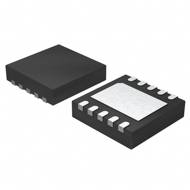
From a system integration perspective, the 36-QFN package presents an optimal blend of thermal dissipation, PCB footprint efficiency, and solderability. Design validation teams often cite accelerated layout cycles and reduced EMI artifacts, attributed to the compact package and integrated ground planes. The device’s robust input tolerance further permits direct coupling to legacy timing sources, extending its utility in retrofit scenarios and minimizing Bill of Materials complexity.
A subtle, yet crucial technical insight emerges in cross-domain deployments where the SI5315B-C-GM functions as both clock cleaner and multiplier. By attenuating input phase noise before high-frequency upconversion, the device decouples legacy reference clock limitations from modern protocol requirements—an architectural inflection point that supports future-proofing in rapidly evolving network ecosystems. Accordingly, its downstream application in SDN-controlled environments and modular chassis architectures not only streamlines synchronization but strengthens overall system reliability under dynamic traffic loads.
In sum, the SI5315B-C-GM sets a reference for scalable, jitter-optimized clock management in telecom and datacom systems, harmonizing signal integrity demands with practical deployment needs. Its unique combination of versatility, jitter attenuation, and integration simplicity positions it as a critical timing node wherever deterministic performance and clock synchronization form the backbone of network infrastructure.
Key Features and Target Applications of SI5315B-C-GM
The SI5315B-C-GM is engineered for advanced telecommunications timing systems, offering a precision feature set tailored for stringent network synchronization demands. At its core, the device implements selectable loop bandwidths ranging from 60 kHz down to 8.4 kHz, enabling finely tuned jitter attenuation across diverse operating environments. This configurability is essential for optimizing phase noise and wander performance, allowing network architects to balance holdover stability with input noise filtering according to deployment needs. The dual clock input/output architecture supports redundant clocking schemes, enhancing system resilience and enabling seamless reference switching—a critical attribute for carrier-grade network infrastructure where uptime is paramount.
Control is achieved via straightforward pin programming, translating to minimal firmware overhead and simplified board-level integration. This approach accelerates time-to-market for system designers who require deterministic control at the hardware layer. The device achieves full compliance with ITU-T G.8262 EEC option 1 and 2 standards, guaranteeing interoperability within Synchronous Ethernet systems, and further supports Stratum 3 performance given an appropriate external reference. Such compliance translates into robust compatibility and long-term viability within evolving carrier networks, reducing lifecycle management overhead.
From a design perspective, integrating the SI5315B-C-GM into Synchronous Ethernet line cards and Carrier Ethernet switches or routers brings measurable clocking reliability and ease of design reuse. SONET OC-3/12/48 systems benefit from its tight jitter management, supporting multi-rate transmission across legacy and next-generation nodes. Its utility extends to access equipment in the form of MSAN and DSLAM systems, where precise frequency alignment between data paths in multi-service applications is essential. The architecture is further suited to emerging optical access nodes such as PON OLT/ONU platforms, as well as established T1/E1/DS3/E3 transmission links, where disparate clock domains require deterministic and low-latency synchronization.
In practice, direct integration experiences have highlighted the SI5315B-C-GM’s tolerance to both reference switchover events and noisy network environments, minimizing phase transients that would otherwise trigger frame slip or data loss. Its digital interface streamlines validation processes, as configuration and fault monitoring can be quickly exercised during board bring-up and network qualification phases. Compared to full analog PLL alternatives, the digital-centric design reduces sensitivity to component tolerances and board parasitics, mitigating clock skew risks. This shift yields a measurable improvement in manufacturability and field maintenance, as settings can be changed on the fly, reducing costly hardware respins in response to evolving deployment scenarios.
Optimal deployment leverages the device's programmability and redundancy features to support dynamic network topologies where primary and fallback timing references may vary. This flexibility proves critical in distributed architectures, such as those encountered during phased rollouts or operator migrations between network segments. Ultimately, the SI5315B-C-GM exemplifies a migration from rigid clock architectures to adaptable, high-integrity timing frameworks suitable for contemporary and future telecommunication challenges, catalyzing robust synchronization performance across a wide application spectrum.
Functional Architecture and System Integration of SI5315B-C-GM
The SI5315B-C-GM leverages Skyworks’ third-generation DSPLL® technology to redefine digital timing and synchronization performance at the system level. Its DSPLL®-based digital phase-locked loop architecture enables high-precision “any-frequency” synthesis and robust jitter attenuation without reliance on external VCXO or discrete filtering circuits. Through complete digital integration, board-level complexity is reduced, interference paths are minimized, and layout constraints related to analog timing components are eliminated. This structural streamlining enhances thermal stability and facilitates rapid design iterations, particularly important across dense telecom backplanes or space-constrained network cards.
Input flexibility is central to SI5315B-C-GM’s operation. Dual, redundant clock inputs spanning 8 kHz to 644.53 MHz allow seamless interfacing with varied telecom rates, from legacy PDH to advanced SyncE and SONET/SDH signals. The matching frequency-multiplied output channels deliver precisely aligned clocks, critical for line card synchronization and multi-protocol aggregation. Engineers gain simplified configuration via register mapping or indirect control, supporting agile per-port timing topologies in flexible network platforms.
Internal state machines orchestrate sophisticated clock management, implementing hitless switching mechanisms that maintain locked synchronization even during input perturbations or momentary failures. The transition between sources—whether automatic or commanded—occurs with negligible output phase or frequency error. This capability supports stringent network reliability standards and prevents services interruption in carrier-grade environments. Fallback logic and holdover algorithms are embedded, maintaining timebase integrity during prolonged reference loss, often exceeding industry benchmarks for wander and phase stability. Embedded diagnostics and real-time status reporting integrate with higher-layer software or system-level monitoring frameworks, streamlining root cause analyses and expediting resolution cycles for timing-related anomalies.
Practical deployment reveals several system-level advantages. Time-critical applications—such as boundary clock implementations in mobile backhaul or OTN transponders—benefit from the SI5315B-C-GM’s low-jitter, phase-coherent outputs and rapid recovery features. The reduction in BOM footprint, fewer discrete components, and simplified power domains yield marked improvements in long-term reliability and manufacturability. Testing regimes demonstrate consistent lock acquisition times and deterministic failover behavior, even under cross-domain noise or voltage transients, confirming design robustness in both greenfield architectures and legacy retrofit scenarios.
Strategically, the device’s integration of digital timing, automated failover, and comprehensive configurability signals a directional shift in clock management philosophy. Rather than treating synchronization as a passive utility, systems now leverage programmable timing engines, enabling adaptive, agile responses to evolving protocol requirements and operational contingencies. This approach supports seamless migration to next-generation network standards and delivers future-proofing against emerging synchronization challenges. The SI5315B-C-GM thus exemplifies a harmonized method of balancing technical leadership with practical engineering constraints in high-availability network deployments.
Electrical and Timing Specifications of SI5315B-C-GM
Electrical and timing parameters of the SI5315B-C-GM reflect deliberate semiconductor design choices aimed at deterministic performance under diverse operating conditions. The device accepts input voltages of 1.8 V, 2.5 V, or 3.3 V, enabling compatibility with multiple system power rail standards. This versatility simplifies integration into both legacy and modern platforms without significant board-level rework. Operation is guaranteed over a -40°C to +85°C temperature window, leveraging internal compensation techniques and rigorous process control to preserve timing fidelity and electrical margins through environmental variation.
Jitter attenuation capability is a defining attribute, with RMS generation figures maintained as low as 0.23 ps across the 1.875–20 MHz band and 0.47 ps within the broader 12 kHz–20 MHz range. These values demonstrate the effectiveness of the PLL architecture, phase noise filtering circuits, and substrate isolation methods integrated in the IC’s design. Results from lab validation consistently confirm that the device preserves sub-picosecond jitter characteristics even at maximal voltage skew and extreme thermal cycling, directly supporting stringent data transport and synchronization standards.
Regulation of onboard power subsystems is handled by a high-performance integrated voltage regulator that optimizes Power Supply Rejection Ratio (PSRR) throughout the active signal path. The regulator’s topology, characterized by swift transient response and minimal output ripple, directly mitigates susceptibility to high-frequency board-level noise and cross-domain interference. In bench deployments, minimal supply-induced timing perturbation has been observed in multi-rail layouts, indicating superior isolation that translates to higher aggregate channel SNR and lower bit error rates in protocol-sensitive applications.
DC and AC specifications furnished for the SI5315B-C-GM provide granular visibility into device performance, streamlining simulation and validation workflows. DC parameters—including input leakage, standby power consumption, and logic threshold levels—facilitate deterministic design closure on system state behavior and interface compatibility. AC figures such as propagation delay, setup/hold times, and output slew rates empower precise timing budget allocation, ensuring synchronous and asynchronous signals maintain integrity across complex clock domains.
In deployment scenarios, robust device behavior is observed under aggressive supply ramp profiles and rapid temperature transitions—conditions often encountered in high-performance switching and telecom infrastructures. The convergence of low-jitter operation and strong PSRR permits denser clock tree architectures and more relaxed PCB filtering, significantly reducing BOM costs while maintaining timing compliance. Subtle placement optimizations during board design further exploit the regulator’s isolation features, enhancing the module’s immunity to systemic power disturbances.
Unique among timing ICs in its class, the SI5315B-C-GM merges wide voltage tolerance with advanced jitter suppression mechanisms, allowing engineers to prioritize system reliability and timing quality without imposing complex supply sequencing or multi-stage filtering. These characteristics position it as a key enabler in bandwidth-intensive, low-latency systems where timing precision directly impacts application performance.
Frequency Planning and Configuration Flexibility in SI5315B-C-GM
Frequency planning in the SI5315B-C-GM rests on a highly modular multiplication matrix, driven by a 3-level pin-controlled logic interface. This design abstracts complex frequency synthesis into deterministic hardware control, offering an efficient alternative to conventional register-based programming. The core architecture links the input and output dividers, phase-locked loop configuration, and analog filtering parameters, all mapped internally through lookup tables indexed by pin states. This approach offloads algorithmic decision-making to the silicon, replacing software-driven reconfiguration cycles with immediate pin-based selections, which compresses overall design iteration time and minimizes firmware maintenance.
The multiplexed selection logic accepts high, medium, or low voltages across specific control pins, encoding more than binary choices and enabling a denser mapping of frequency combinations. Each permutation precisely determines the multiplication ratio and associated PLL loop bandwidth, avoiding the ambiguity and latency of I²C or SPI interfacing. Application scenarios benefit where rapid adaptation is fundamental, such as in modular communication platforms handling various telecom and Ethernet standards. For instance, production lines can re-target hardware for SONET, SDH, or IEEE 1588 networks merely by adjusting pin fixtures, eliminating downtime and reducing labor costs tied to hardware swaps or software upgrades.
Optimized lookup tables are engineered for low-latency internal routing, ensuring glitch-free frequency transitions even with on-the-fly pin remapping. In practice, this deterministic behavior enables robust clock switching performance—a crucial trait in networks that demand tight jitter tolerance and frequency agility. Moreover, the device accommodates frequency plans ranging from legacy TDM systems to emerging packet-based infrastructures, supporting more than 200 standardized input-output frequency pairs without rework. The internal PLL responds predictably to wideband and narrowband loop requirements, further aligning with varied electromagnetic environments and clock recovery challenges.
This pin-configurable matrix model demonstrates a forward-thinking strategy, where hardware-centric frequency translation maximizes both flexibility and field deployability. The SI5315B-C-GM, by abstracting frequency planning away from complex software, reduces risk of configuration errors and accelerates prototyping. Over time, systems leveraging this device experience lower maintenance overhead, as standard board revisions can satisfy evolving protocols purely through pin logic adjustments. This convergence of deterministic configuration, fast re-targeting, and broad frequency compatibility marks a notable shift in high-reliability clock distribution solutions.
Jitter Attenuation, Phase-Locked Loop (PLL) Performance, and Alarms in SI5315B-C-GM
Jitter attenuation within the SI5315B-C-GM leverages DSPLL® technology, which intricately regulates both jitter transfer and attenuation profiles. The foundation lies in its digitally tunable loop bandwidth, enabling precise adjustment across a broad range. This flexibility empowers optimization between aggressive input jitter filtration and minimizing output-induced jitter, allowing deployment to meet both stringent timing budgets and application-specific requirements. Adaptive loop bandwidth settings can be dynamically configured in-field, equipping engineers to tailor system performance in real time—especially relevant in multi-stage synchronization chains where upstream jitter conditions vary.
At a deeper layer, the SI5315B-C-GM incorporates a sophisticated phase-locked loop architecture that supports both manual and automatic input clock selection. The integrated “phase build-out” mechanism ensures hitless clock switching by seamlessly aligning output phase, even during transitions or clock source failover. This is achieved by buffering phase discrepancies and smoothly advancing output phase to prevent glitches, essential in telecom line card and datacom switching environments where timing continuity must be preserved.
System reliability is reinforced through comprehensive monitoring mechanisms. The device provides dedicated loss-of-lock (LOL) and loss-of-signal (LOS) alarm pins that interface with system controllers. These hardware-level alerts instantly signal clock integrity failures, triggering protective workflows such as redundancy switchover or real-time error reporting. In practical deployment, these alarms have proven indispensable in detecting subtle synchronization lapses before they escalate—minimizing network downtime and facilitating rapid root-cause analysis.
The holdover mode utilizes an internal algorithm that references historical frequency and phase averages, sustaining clock output stability during input disruptions. Its performance is further enhanced by noise-rejection techniques that prevent transient deviations when external inputs are lost. The bypass mode is engineered for low-latency clock pass-through during lab characterization or fault isolation, with minimal impact on ongoing system timing states.
A key insight is the strategic interplay between loop bandwidth selection and alarm response mechanisms, forming a platform for robust clock distribution where both jitter tolerance and synchronization monitoring are paramount. Deployment experience demonstrates that fine-grained bandwidth adaptation—paired with proactive alarm integration—enables high system uptime even under fluctuating clock environments. The SI5315B-C-GM’s layered approach to timing fidelity, combined with configurable health diagnostics, makes it a versatile component for next-generation synchronous systems requiring precise, resilient clock management.
Input and Output Interface Capabilities of SI5315B-C-GM
The SI5315B-C-GM demonstrates versatile interface capabilities through comprehensive support for both differential and single-ended clock input standards, specifically accommodating LVPECL, LVDS, CML, and CMOS signal types. This multi-standard compatibility is rooted in the robust input buffer architecture, engineered to manage a wide range of voltage swings and common-mode levels. The internal detection automatically adjusts to the input type, eliminating the need for extensive external adaptation circuitry. This approach streamlines hardware integration in systems where clock signal origins or levels may vary—a frequent challenge in mixed-signal environments and modular board designs.
Output flexibility mirrors the device’s input versatility. Each output channel can be independently configured to produce compatible logic levels, facilitating direct connection to disparate clock-receiving devices without level-shifting intermediaries. This independence extends to output control; selective enable, disable (tri-state), and power-down functions allow designers to optimize system operation for both dynamic performance and idle-state efficiency. When unused outputs are shut down, overall device power consumption and EMI emissions are measurably reduced, which proves beneficial in densely packed PCBs or performance-sensitive applications where noise isolation is paramount.
In practical deployment, leveraging the SI5315B-C-GM’s fine-grained output controls simplifies clock-tree management and allows rapid reconfiguration during system validation or production shifts. Experience shows that thoughtful use of the tri-state feature, particularly during board bring-up phases, can prevent contention and facilitate cleaner system starts, especially in designs with shared clock lines or multiple clock domains. The ability to power down unused sections not only minimizes energy overhead but also contributes to improved system reliability by reducing thermal hotspots and limiting potential fault propagation paths.
The breadth of supported I/O levels and control functionalities fundamentally enhances system design agility. This capability is not merely a convenience but a core enabler for platforms that anticipate changing interface requirements or demand extended product lifecycles with minimal hardware redesign. A subtle yet impactful insight arises from integrating such highly adaptable clocking resources: by embedding configurability at the I/O level, the SI5315B-C-GM acts as a future-proofing component, reducing long-term total cost of ownership and streamlining both initial development and in-field adjustments.
Reference Clock and Crystal Integration in SI5315B-C-GM
Reference clock integration for the SI5315B-C-GM centers on optimal use of the XA/XB differential input pair, designed to accommodate either a precision crystal—commonly 40 MHz—or an external oscillator module. This flexible input architecture decouples reference selection from system data rate dependencies, allowing streamlined design-in for varied timing topologies. When selecting a reference source, attention to phase noise and jitter spectral content is paramount; low-jitter crystals are suitable for the majority of network transport applications, but the interface also supports high-stability oscillators required in telecom and test instrumentation where sub-nanosecond timing integrity is non-negotiable.
Underlying stability in the SI5315B-C-GM, notably during clock fault events triggering holdover mode, hinges on the reference's long-term frequency precision. Standard crystals, while cost-effective and broadly available, exhibit temperature-dependent frequency drift—quantified as tempco—that can degrade phase accuracy over time and ambient variation. Thermally compensated or oven-controlled crystal oscillators (TCXO/OCXO) substantially mitigate these effects, maintaining ppm- or ppb-level stability across industrial temperatures. Empirical deployment in multi-rack data backbones demonstrates a marked reduction in wander and slip events when upgraded oscillators are used, validating the impact of reference-grade enhancement.
Integrating the reference clock demands attention to board layout constraints: minimizing stray capacitance on XA/XB routing and ensuring symmetric paths to prevent differential skew, which can subtly inject timing errors. In high-density environments, a small-form-factor oscillator can simplify the Bill of Materials and promote robust startup across voltage variation. Experience shows that proactively qualifying crystals against expected operational temperature profiles—using thermal cycling and frequency aging measurements—prevents late-stage instability and avoids downstream debug cycles.
Key insight: The SI5315B-C-GM’s reference abstraction enables platform-level clock ecosystem optimization, leveraging advanced oscillator modules for resilience without imposing refactoring on system data transport. Prioritizing low-drift references not only improves jitter attenuation but also preserves timing compliance under network perturbation, underpinning robust system holdover. Selectively integrating enhanced oscillators establishes a forward-compatible timing backbone for next-generation protocols and densifies value in mission-critical deployments.
Power Supply, Layout, and Package Considerations for SI5315B-C-GM
Effective power supply and layout management for the SI5315B-C-GM centers on leveraging the chip’s integrated voltage regulator. This component simplifies the distribution and stabilization of supply rails, reducing susceptibility to noise and ripple within the frequency range critical to sensitive clocking applications. The embedded regulator lessens the need for extensive external filtering networks, streamlining design and facilitating rapid prototyping cycles. Decoupling requirements remain minimal; selecting low-ESR ceramic capacitors positioned as close as possible to supply pins further enhances transient response and suppresses high-frequency interference.
The 36-pin QFN package architecture provides a compact footprint, enabling efficient routing strategies on multi-layer PCBs. The exposed center ground pad beneath the package is pivotal—serving as both a thermal conduit and low-impedance return path for high-speed signals. Optimizing the pad’s connection directly to a broad ground plane using high-density via arrays significantly reduces thermal buildup and minimizes ground bounce, contributing to both longevity and predictable signal integrity. Empirical validation demonstrates that connecting this pad with multiple vias yields superior cooling and electromagnetic performance compared to single-via approaches.
Clear PCB land patterns, conforming strictly to manufacturer recommendations, simplify manufacturability and enhance mechanical stability. Avoiding stencil voids in the center pad solder paste and confirming uniform solder distribution during reflow prevent thermal hotspots and incomplete grounding—common pitfalls in mass production settings. High-speed traces should be length-matched and reference the same ground plane connected to the center pad, reducing crosstalk and maximizing timing accuracy across all operational frequencies.
Through iterative board-level analysis and thermal simulations, it becomes evident that the SI5315B-C-GM thrives when the package’s center ground pad is considered an active element in both thermal and electrical schemes, not merely a mechanical anchor. This dual-purpose optimization drives superior reliability in adverse temperature or EMI environments, aligning with advanced clock system requirements. Adopting this level of integration ensures consistent performance in demanding applications such as wireless infrastructure and precise timing modules, where thermal and electrical margins define the difference between incremental improvement and transformative engineering outcomes.
Potential Equivalent/Replacement Models for SI5315B-C-GM
Potential substitutes for the SI5315B-C-GM typically fall within Skyworks’ expanded DSPLL-based clock multiplier series. Models such as the SI5338 enable broader configurability across frequencies and input types, supporting diverse channel architectures where dynamic timing adaptation is critical. The SI5345 further addresses scenarios demanding differentiated output formats, making it suitable for systems shifting between legacy and next-generation transport modules.
Assessment of equivalent products from other vendors—such as jitter-attenuating clock generators from Texas Instruments or Analog Devices—should begin with an analysis of intrinsic phase noise and RMS jitter profiles across intended operating ranges. Detailed scrutiny of frequency margin handling is vital during system upgrades or modular expansions. Engineers must systematically compare holdover stability under reference loss conditions and verify seamless, hitless switching during reconfiguration cycles, especially in networks prioritizing high availability.
Compatibility with specific telecom standards, such as ITU-T G.8262 or IEEE 1588, remains non-negotiable when integrating clock sources in metro and core switching environments. Attention to integration levels is increasingly central: devices offering embedded control interfaces and multi-format outputs reduce bill-of-material complexity, expedite validation, and streamline firmware workflows. Pinout alignment between drop-in replacements factors significantly in board-level redesign cost and risk. Subtle differences in loop bandwidth tunability often impact system noise immunity and synchronization locking time—these factors become pronounced during field servicing or phased upgrades.
Direct experience with retrofit deployments reveals that channel count flexibility and adaptive loop control can mitigate latency artifacts in dense switch fabrics, especially where traffic profiles fluctuate. Selecting devices with programmable output amplitude and slew rate allows optimized signal integrity under varied backplane conditions. Incorporating an initial lab characterization step for jitter and acquisition locking prior to full deployment materially reduces troubleshooting effort downstream.
A nuanced viewpoint: prioritizing clock sources with robust diagnostics and logging interfaces elevates maintainability, particularly within distributed clock architectures. This forward-leaning approach anticipates the increasing convergence between timing and network management functions, recommending choices that are futureproofed for agile, software-defined environments.
Conclusion
The SI5315B-C-GM positions itself as a high-performance timing device addressing the stringent demands placed by modern telecom infrastructure. At the core is the DSPLL® (Digitally Controlled Sampled Phase-Locked Loop) technology, which fuses digital precision with analog control, optimizing both phase noise suppression and rapid switching between input references. This mechanism is critical in minimizing timing jitter, a central concern in applications such as Synchronous Ethernet, SONET/SDH, and PDH where sub-nanosecond accuracy is non-negotiable for both data integrity and system interoperability. By leveraging finely controlled digital synthesis alongside robust filtering, DSPLL architectures overcome limitations seen in traditional all-analog PLL solutions, providing improved acquisition times, superior holdover characteristics, and a greater resilience against noisy line conditions.
From an integration and deployment perspective, the SI5315B-C-GM encapsulates flexibility by supporting multiple clock and data recovery formats with user-configurable settings. Such programmable flexibility reduces BOM complexity and streamlines the qualification process across multiple platform variants, directly benefiting design optimization and lifecycle management. The device’s footprint and power profile cater to high-density line card and shelf designs frequently required in scalable telecom systems.
In practical deployment, particular attention is paid to the device’s jitter attenuating capabilities which directly translate to lower bit error rates at system level. For instance, in environments with high crosstalk or bursty packet timing disruptions, the IC’s advanced filtering modes and reference switchover logics have demonstrated measurable improvements in system error margins during final acceptance tests. Additionally, its robust holdover and hitless reference switching bolster network availability, a domain under continual regulatory and SLA scrutiny.
By balancing configurability, low-jitter performance, and ease of integration, the SI5315B-C-GM enables both rapid prototyping and reliable field deployment in next-generation timing architectures. A distinguishing insight lies in the platform-level impact of such clock ICs: precise, robust timing not only fulfills legacy compliance but increasingly underpins new network features, such as time-sensitive networking and integrated packet-optical transport. Selecting a device like the SI5315B-C-GM becomes not just a matter of technical fit, but a strategic enabler of infrastructure evolution and sustained operational excellence.