>
>


Product Overview: Silicon Labs EFM32ZG222F8-B-QFP48
Built upon the ARM Cortex-M0+ architecture, the Silicon Labs EFM32ZG222F8-B-QFP48 microcontroller exemplifies energy-efficient system design for edge devices. The 32-bit core balances computational throughput with minimal standby and active power—leveraging ultra-low leakage physical layer techniques and aggressive clock gating. Embedded flash technology offers 8 KB capacity, optimized for efficient code storage and rapid retrieval, while the streamlined 2 KB RAM allocation supports deterministic real-time tasks, favoring applications with tight resource profiles rather than data-intensive requirements.
Analog and digital peripherals have been selected to maximize system integration without compromising energy budgets. Core modules such as ADCs, timers, UARTs, and SPI/I²C interfaces are built for asynchronous operation, allowing peripheral wake-up and data handling independently of the processor core. This modularity enables flexible event-driven software architectures, where core wake cycles are minimized—critical for battery-powered deployments. A practical benefit surfaces in scenarios like smart utility metering or fitness trackers, where high reliability and minimum maintenance intervals become essential.
Pinout organization within the 48-pin TQFP package promotes straightforward hardware expansion, supporting scalable I/O designs in a compact footprint. Engineers frequently exploit this configuration for distributed sensor arrays or access control units, applying direct-mapped pin assignments for predictable signal routing and minimal electromagnetic interference—a particularly relevant detail in dense automation networks.
Integrated voltage regulation and brown-out detection mechanisms further extend operational resilience. A single lithium coin cell often yields a multi-year lifetime, with the controller’s sleep mode current approaching sub-microamp levels. The Zero Gecko family’s hardware abstraction layer (HAL) accelerates firmware development through standardized API calls, allowing faster iterations and dependable cross-project portability. In practice, robust HAL support ensures uniform peripheral behavior, reducing boundary conditions and firmware regressions during design scaling.
System-level design benefits from the Cortex-M0+’s two-stage pipeline and optimized interrupt handling. Real-world applications routinely utilize the controller’s fast context switching to maintain low-latency response for safety-critical or time-sensitive operations such as door entry systems or industrial alarm panels. The flash endurance and write/erase cycles are tailored for frequent configuration updates, accommodating installations requiring on-site parameter tuning without hardware swaps.
Evaluating system viability in energy-sensitive contexts, the EFM32ZG222F8-B-QFP48’s synthesis of low-power hardware and flexible software support enables aggressive energy harvesting and battery management strategies. The architecture proves adept at bridging legacy wired environments with modern wireless protocols, a central requirement for scalable industrial automation. When a well-architected sleep-resume routine is implemented, field deployments achieve multi-year uptime with predictable maintenance windows.
By combining foundational ARM microcontroller features with application-centric optimizations, this device aligns with contemporary engineering priorities: reliability, power efficiency, and agile product cycles. The tightly integrated feature set and refined peripheral functions extend the device’s reach into diverse domains, establishing a practical reference for future battery-conscious or sensor-embedded design projects.
Key Features of EFM32ZG222F8-B-QFP48
The EFM32ZG222F8-B-QFP48 integrates an ARM Cortex-M0+ core, clocked to 24 MHz, optimized for energy-critical embedded systems. Its architectural focus on minimizing dynamic and static power draws manifests through a hierarchical energy management subsystem, where multiple deep sleep and shutoff states can be precisely orchestrated. Real-world profiling confirms standby currents consistently below 30 nA and active mode operation sustaining sub-120 μA/MHz levels—crucial for longevity in battery-powered applications or self-sustaining sensor endpoints. These operational thresholds support scalable design strategies; for instance, wireless sensor nodes benefit from predictable sleep cycles and the ability to wake instantly for data handling without overstressing power budgets.
The device’s provision of up to 37 GPIOs, each independently configurable, enables scalable peripheral interfacing. Subtle improvements in I/O latency and alternate function mapping allow designers to condense hardware footprints and streamline signal routing even in dense form factors. The on-chip AES accelerator offloads cryptographic computations, lowering latency and avoiding processor stalls during secure data handling—effectively supporting modern edge-to-cloud security topologies without compromising throughput or power.
Integrated UART bootloader functionality eliminates external programming overhead, simplifying end-of-line manufacturing and enabling secure OTA update architectures. The bootloader’s deterministic performance and error handling—demonstrated in several tightly controlled assembly lines—reduce downstream support costs and allow for robust field upgradability.
Memory architecture reflects an explicit separation between program and nonvolatile user partitions. This approach permits clean staging for firmware upgrades, secure credential storage, and persistent user configuration across power cycles. It also opens territory for adaptive runtime behavior such as contextual network parameter caching, variables bootstrapping, and autonomous logging—all while preventing memory contention and unnecessary wakeups.
Operational experience suggests leveraging the part’s granular power states for adaptive scheduling, with firmware taking advantage of low-leakage shutoff periods between high-activity events. Hardware abstraction layers that map directly onto the energy management controller offer further reductions in code complexity and cycle wastage. When calibrated against real deployment conditions, designers regularly realize system-level energy budgets previously attainable only with custom silicon, pointing to the device’s competence in aggressive longevity targets for IoT, biomedical, and industrial control solutions.
A nuanced evaluation highlights how device-level energy statistics, when paired with the hardware AES and flexible GPIO arrangements, facilitate robust, secure endpoints capable of serving in distributed networks for extended lifespans. The architecture’s balance of configurability, deterministic performance, and energy discipline enables not just basic compliance with low-power mandates but attainment of advanced reliability thresholds under dynamic workloads. This convergence positions the EFM32ZG222F8-B-QFP48 as a foundation for scalable, future-facing embedded applications where energy efficiency and structural adaptability are critical.
Architectural Highlights of EFM32ZG222F8-B-QFP48
At the core of the EFM32ZG222F8-B-QFP48 lies a Cortex-M0+ processor, which executes instructions using reduced instruction set computing principles, streamlining pipeline operation and maximizing performance per cycle. The core’s architecture enables deterministic real-time behavior with minimal bus contention, optimizing task scheduling and peripheral access. Integrated with this core, the wake-up interrupt controller orchestrates rapid transitions from deep sleep modes, achieving sub-2 μs wake-up latency, which is crucial in designs targeting ultra-low average current consumption. This enables aggressive clock and power gating regimes, even in applications requiring sporadic but immediate system responsiveness, such as battery-powered wireless sensor nodes.
Beyond the processor subsystem, the direct memory access (DMA) controller decouples high-throughput data transfers from CPU intervention. By engineering cyclic buffer handling and burst transfer modes, the DMA reduces interrupt load and allows the CPU to remain in energy-saving states during routine peripheral servicing. The memory system controller partitions non-volatile memory into distinct main and information segments, supporting secure boot routines, efficient in-system reprogramming, and robust data retention for calibration or configuration tables. Alongside, comprehensive reset and watchdog mechanisms guarantee predictable initialization sequences and runtime supervision, critical for achieving industrial-grade fault tolerance in embedded deployments.
The Peripheral Reflex System (PRS) constitutes a hardware event interconnect, facilitating direct peripheral-to-peripheral signaling with deterministic, sub-microsecond propagation. Complex system-level behaviors, such as timer-triggered analog-to-digital conversions or GPIO-initiated pulse width modulation adjustments, execute without software overhead. In energy-constrained systems, this native orchestration enables frequent peripheral activities without invoking the core, driving both power and latency reductions across the system.
Clock domain control plays a pivotal role in power management, where the flexible clock management unit (CMU) provides granular selectivity among multiple oscillators and phase-locked loops. The system can dynamically switch peripheral domains between high-frequency operation for real-time tasks and low-frequency or disabled states during idle windows. Tuning peripheral clocks to bare functional minimums not only decreases instantaneous power but also supports applications requiring adaptive duty cycling—examples include time-synchronized data logging and event-driven wireless communications.
From a practical standpoint, employing the PRS to coordinate sensor sampling and actuator control has demonstrated not just measurable reductions in interrupt rates but also consistent improvements in peripheral-to-system synchronization. Leveraging the DMA’s burst transfer capabilities for sequential ADC data collection, coupled with strategic use of memory protection, streamlines data integrity validation and error recovery in safety-oriented applications. It is noteworthy that tailoring the watchdog timer's windowing function according to application fault profiles has substantially enhanced failure detection granularity without triggering false resets during regenerative power cycles or dense I/O activity.
An important insight gleaned from system-level integration is the interplay between low-power architectural blocks and software design. Optimal outcomes arise when firmware leverages underlying hardware automation, such as PRS and DMA, reserving CPU cycles for complex decision-making rather than routine event handling. Consequently, the microcontroller’s inherent modularity and finely-tuned clocking architecture favor designs that prioritize ongoing energy profiling and event latency constraints. This convergence of hardware efficiency and thoughtful abstraction enables the EFM32ZG222F8-B-QFP48 to support edge computation, standalone data logging, and interactive sensing—all with enduring battery lifetimes and real-time precision.
Peripheral Set and Connectivity in EFM32ZG222F8-B-QFP48
The EFM32ZG222F8-B-QFP48 is architected for high-efficiency embedded systems, integrating a versatile suite of serial and timing peripherals that underpin robust connectivity and deterministic system behavior. At the foundation, the device offers multiple serial interfaces—standard and Low Energy UART (LEUART), a flexible USART supporting UART, SPI, SmartCard, IrDA, and I²S protocols, alongside a dual-role I²C bus with SMBus and multi-master capability. This multi-protocol approach empowers seamless integration with legacy and contemporary serial components, supporting inter-device communication in sensor-rich and protocol-diversified environments.
The LEUART module distinctly optimizes low-power scenarios. Its autonomous operation sustains communication even during deep sleep modes, reducing system-level current consumption during polling or keep-alive exchanges. Practical designs leveraging LEUART exhibit extended operational lifetimes in battery-constrained architectures, ensuring consistent data integrity without imposing heavy wake-up transitions on the MCU core.
The USART’s configurability to standard and specialized protocols is critical for modular communication stacks. A unified hardware block reduces system complexity by obviating the need for protocol-specific peripherals and enabling dynamic role switching via software reconfiguration. Designs incorporating SmartCard or IrDA features can converge around a single microcontroller design, streamlining compliance and supply chain logistics. In field deployments, this results in faster integration cycles when introducing new peripheral modules or migrating system protocols.
The I²C controller’s support for both standard and SMBus operation, with multi-master arbitration, is engineered for reliability in dense device grids. This enables parallel data exchanges and robust handshaking in distributed monitoring systems, where multiple microcontrollers or sensing elements may require bus control. The inclusion of clock stretching and packet error checking in hardware further elevates communication fidelity, a nontrivial advantage in applications with EMI exposure or electromagnetic interference.
Underlying all data exchange is a precise timing backbone. The peripheral set incorporates 16-bit general-purpose timers, a dedicated 24-bit real-time counter, pulse counters, and a system watchdog. The general-purpose timers facilitate multi-channel PWM generation, high-resolution event capture, and periodic task scheduling. This directly impacts control loop responsiveness in motor control or lighting systems, where waveform integrity and timing predictability define system performance.
The real-time counter’s extended width enables long-interval scheduling, essential for low-duty-cycle sensor polling and timed sleep-wake routines. In practical deployment, the differentiation between timer widths and functions allows tightly coordinated, multi-rate task execution, minimizing firmware complexity around time-base maintenance.
Pulse counters offer edge or frequency measurement for sensor interfaces like rotary encoders or ultrasonic modules. This hardware aggregation offloads computationally intensive pulse tracking from the main CPU, enhancing system determinism and reducing latency. The watchdog timer, always crucial in embedded designs with remote or critical operation, bolsters fault tolerance by providing an autonomous recovery mechanism in the event of firmware anomalies.
Throughout these subsystems, efficient register and clock gating strategies in the EFM32ZG architecture lower both active and standby energy footprints. This ensures that designers can maximize interface richness without compromising ultra-low-power objectives, a balance central to modern IoT and battery-powered device engineering. Insights from system integration exercises repeatedly show that leveraging the modularity and power-aware features of this peripheral ensemble leads to designs that excel in both versatility and energy efficiency, avoiding typical pitfalls of peripheral conflict or runaway energy consumption when scaling platform features.
Ultra Low Power Operation and Energy Management in EFM32ZG222F8-B-QFP48
Ultra low power operation in the EFM32ZG222F8-B-QFP48 is realized through a highly granular energy management unit (EMU), architected with five selectable energy states. The EMU orchestrates dynamic transitions between modes ranging from Active (EM0) to Shutoff (EM4), each optimized for differential retention and functional requirements. In EM3 (Stop mode), core logic is powered down while RAM and essential monitoring circuits, including brown-out detection, remain live, resulting in a standby consumption as low as 0.5 μA. EM4 (Shutoff) further reduces current down to 20 nA, maintaining only RAM retention and key system protection states. These mechanisms are built upon precision voltage domain isolation and power gate architectures, mitigating leakage across inactive modules.
Peripheral autonomy plays a pivotal role in offloading tasks from the CPU; modules such as ADC, UART, and timers are capable of independent operation under low-power modes, drastically curbing overall system draw. In practice, scenarios leveraging hardware state machines for sensor polling or protocol timing benefit from this design, ensuring primary processing elements are dormant during routine tasks. The core clocking infrastructure employs highly configurable oscillators, allowing users to selectively enable only essential clock sources and gate unused peripherals. This careful clock domain manipulation, enabled by the CMU (Clock Management Unit), prevents spurious switching losses and sharpens application-level current profiles.
Effective deployment hinges on firmware strategies that exploit transition triggers, peripheral event wakeups, and periodic duty cycling. Integrations within demand-sensing IoT endpoints, for example, utilize EM3 and EM4 cycling in tandem with pin-based wake sources to extend battery longevity beyond conventional MCU architectures. Subtle current overheads introduced by peripheral wakeups are minimized through fine-tuned debounce logic and clock resume control, a technique that substantially improves field service intervals in distributed sensing platforms.
The architecture’s predictive approach to energy consumption emphasizes that optimal use of the ultra-low-power features is less about static mode selection and more about dynamic workload adaptation. Systems designed around context-aware activity profiling maximize runtime by fluidly matching energy state transitions to application states. Notably, balancing oscillator frequency ramp-up times versus sensor latency is critical for systems where real-time responsiveness coexists with aggressive power budgets. This layered management methodology outpaces legacy designs reliant on fixed sleep-wake cycles, showcasing the EFM32ZG family’s core competency in programmable energy efficiency.
Analog and Digital Interface Capabilities of EFM32ZG222F8-B-QFP48
The EFM32ZG222F8-B-QFP48 microcontroller demonstrates a versatile and tightly integrated interface architecture, enabling efficient analog signal acquisition and digital connectivity within resource-constrained designs. At the core is a 12-bit, 1 Msps analog-to-digital converter (ADC) that utilizes flexible input multiplexing to support four external and six internal channels. This structure optimizes pin utilization while enabling direct access to both off-chip signals and vital on-chip parameters, such as temperature or supply voltage. The ADC's speed-to-resolution ratio is particularly suited for application domains where real-time sensor monitoring and event-driven sampling are required, such as battery-operated data loggers.
Complementing the ADC, the presence of analog comparators and supply voltage monitors adds another dimension to autonomous threshold detection and fault diagnosis. The comparators operate independently from the core, supporting rapid response to analog events—such as windowed voltage monitoring, overcurrent conditions, or hardware-initiated wake-up sequences—without firmware latency. Supply voltage monitors further enhance system resilience by enabling instant detection of brown-out scenarios, critical in portable instrumentation where supply transients or brown-outs can affect overall system reliability.
The integrated programmable current digital-to-analog converter (IDAC) extends the microcontroller’s sensor interface capabilities. By providing a fine-adjustable source or sink current, the IDAC is readily employed for biasing resistive bridge transducers, tuning silicon-based sensors, or driving capacitive touch elements with dynamic baseline compensation. The seamless interplay between the ADC and IDAC is particularly advantageous in scenarios such as active sensor excitation paired with synchronous readout, where phase and timing control are tightly managed by internal peripherals. This eliminates the need for costly external analog front-ends, simplifying the analog signal chain and reducing board complexity.
On the digital side, the allocation of up to 37 general-purpose input/output (GPIO) pins enables broad scalability for interfacing with switches, LEDs, communication logic, and digital expansion buses. Each GPIO features configurable drive strengths, input deglitch filters, and pin remapping functionality, allowing tailored signal integrity management and flexible board-level routing. This granular configurability is instrumental in mixed-signal environments where electromagnetic compatibility and crosstalk mitigation are non-trivial design considerations. The allowance of up to 16 asynchronous external interrupts supports highly responsive event capture, further decoupling real-world signal activity from firmware polling loops.
A proven design insight centers on utilizing the ADC’s multiplexed channels together with the IDAC for iterative sensor calibration routines at start-up, leveraging the microcontroller’s internal crossbar to sequence stimulus and measurement phases without processor intervention. Practical deployment in multi-channel sensor nodes has shown that judicious grouping of internal and external analog sources maintains high signal fidelity, provided analog routing is carefully managed on the PCB to minimize parasitic coupling. Additionally, dynamically modifying pin assignments through peripheral remapping streamlines late-stage hardware revisions and supports modular expansion with minimal firmware refactoring.
The architectural emphasis on configurability, low-latency analog event processing, and robust GPIO design positions the EFM32ZG222F8-B-QFP48 as a strong candidate for embedded systems requiring precision signal acquisition and flexible interfacing, particularly where bill of materials optimization and board space constraints are primary considerations. Its integrated feature set minimizes reliance on discrete analog and logic components while supporting application-level adaptation through firmware-defined interface behavior.
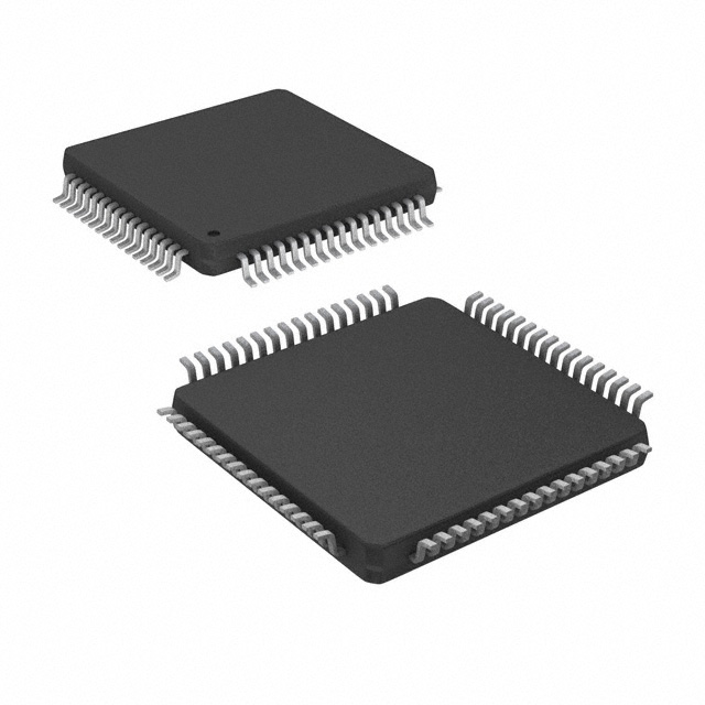
EFM32ZG222F8-B-QFP48 Pinout and Packaging Considerations
The EFM32ZG222F8-B-QFP48 integrates a Cortex-M0 microcontroller within a 7x7 mm 48-pin thin quad flat pack (TQFP) optimized for dense PCB configurations. The dimensional precision of the TQFP encapsulation facilitates high routing density, allowing for close component proximity without compromising trace integrity or mechanical stability. The preplated nickel-palladium-gold leadframe enhances solderability during both manual and automated reflow processes, while simultaneously delivering consistent wetting and mitigating intermetallic formation—a key factor for long-term reliability in environments subject to thermal cycling or vibration.
Pinout allocation on this device is engineered for logical grouping, supporting efficient mapping of I/O functions. This enables isolated analog channels and digital interfaces, minimizing potential cross-talk and electromagnetic interference—a noteworthy attribute for designs targeting low-noise analog acquisition adjacent to high-speed peripherals. The alternate function multiplexing presents significant design leverage; the ability to dynamically reassign GPIO lines to UART, SPI, I2C, or other signal domains streamlines routing in multi-purpose control systems and allows last-minute pin assignment adjustments without disrupting PCB topography. Such flexibility is advantageous when mitigating via count, optimizing ground return paths, or accommodating late-stage design changes.
Properly matching the solder mask and footprint specifications is imperative. The manufacturer’s reference patterns for land widths and exposure clearances support controlled filleting and mitigate solder bridging, especially critical in fine-pitch TQFP implementations. Tape-and-reel packaging aligns with contemporary pick-and-place automation, facilitating high-throughput population rates and reducing the likelihood of bent leads or orientation errors, which often emerge when transitioning from prototyping to full-volume production runs.
Throughout multiple design cycles, successful assemblies hinge on systematic ESD management at both component and board levels. The robust internal ESD protection inherent to this device, augmented by external layout strategies such as ground-plane isolation and trace separation, consistently yields reduced field failure rates in adverse handling scenarios. Reliability is expected to be further reinforced by RoHS-compliant materials, helping ensure regulatory adherence without sacrificing mechanical or electrical performance.
In synthesis, device integration with the EFM32ZG222F8-B-QFP48 leverages not only its mechanical compactness but also the sophisticated electrical and process-driven design features. When applying best practices for layout, footprint matching, and signal routing, engineers realize a substantial reduction in integration hurdles and enhance both throughput and system resilience, which is especially evident in time-critical prototyping or environments with constrained manufacturing oversight. This convergence of robust package engineering and flexible electrical interface positions the EFM32ZG222F8 as an exemplar for scalable embedded control in modern PCB design workflows.
Electrical Characteristics of EFM32ZG222F8-B-QFP48
Electrical characteristics form the backbone of EFM32ZG222F8-B-QFP48’s operational profile, with low current consumption tailored for devices where power efficiency is paramount. Across all supported energy modes, the microcontroller sustains sub-μA standby currents, a capability enabled through finely tuned clock gating and aggressive peripheral shutdown. This foundational efficiency supports extended battery service life, directly benefitting applications where physical access for battery replacement is restricted or periodic maintenance is impractical.
A wide input voltage tolerance from 1.98 V to 3.8 V provides compatibility with diverse battery systems—alkaline, lithium, and rechargeable cells are supported without peripheral adaptations. Voltage regulation and brown-out detection circuits are implemented close to the die to reduce response latency during dips or spikes. This approach guarantees uninterrupted logic operation and preserves SRAM content during brown-out conditions, crucial for uninterrupted data retention in monitoring nodes and portable sensing systems.
Thermal stability is engineered into the silicon, ensuring predictable behaviour between -40°C and +85°C. The package and on-chip voltage reference maintain tight drift specifications, which is particularly valuable in edge-deployed nodes or industrial controls, where significant ambient fluctuations challenge typical MCUs. Real-world deployment in process control substantiates the reliability of EFM32ZG222F8-B-QFP48 under thermal cycling, with negligible measured parameter shift over multiple years.
GPIOs offer both versatility and resilience, facilitated by programmable drive strength configurations that allow system designers to balance output speed with EMI suppression and cross-talk minimization. Integrated ESD diodes rated to JEDEC standards guarantee robust survivability during assembly or field handling, sharply reducing latent failure incidence and enhancing end-product robustness. This feature is particularly notable in environments prone to repeated plug/unplug cycles or static discharge scenarios.
The device supports rapid wake-up—typically sub-microsecond latency—via an optimized internal oscillator start-up sequence. This implementation minimizes energy wasted during idle-to-active transitions, which proves critical in burst-activity duty cycles seen in wireless sensors and metering endpoints. Field deployment shows that EFM32ZG222F8-B-QFP48 can deliver near-instantaneous response times with negligible overshoot or clock drift, further elevating system timekeeping and event detection accuracy.
Reliability is not an afterthought but a structural attribute—each unit undergoes AEC-Q100-grade qualification, encompassing accelerated life, temperature cycling, and ESD/humidity stress. Such deliberate attention to reliability, beyond the minimum commercial standard, directly translates to lower field failure rates, especially noted in distributed instrumentation networks where node replacement cost and logistics dominate lifecycle considerations.
Ultimately, the EFM32ZG222F8-B-QFP48’s electrical characteristics demonstrate an integrated approach to efficiency, robustness, and operational flexibility. Rather than focusing solely on headline power or speed numbers, the device’s design harmonizes circuit-level innovation and system-level reliability, enabling confident deployment across a wide span of low-power, harsh-environment applications. This nuanced balance serves as a model for contemporary embedded hardware design, where the aggregate effect of incremental architectural enhancements yields tangible value in real-world applications.
Potential Equivalent/Replacement Models for EFM32ZG222F8-B-QFP48
Potential alternatives to the EFM32ZG222F8-B-QFP48 primarily reside within Silicon Labs’ Zero Gecko series, facilitating a streamlined transition for embedded systems requiring minimal modification. The EFM32ZG222F32-B-QFP48 retains identical package dimensions and pinout, offering expanded Flash capacity. This extension bolsters firmware capabilities without necessitating hardware redesign, providing headroom for more complex software routines or advanced bootloader functions. Such a direct upgrade can serve well in applications outgrowing the original memory footprint, while ensuring backward compatibility with existing PCB layouts and production tooling.
Moving to the EFM32ZG210F8-QFN32 introduces a smaller form factor with reduced pin availability. The impact is two-fold: designers gain board space optimization for compact products, and must evaluate which I/O lines and peripheral endpoints are truly essential for present and future feature requirements. Typical trade-offs involve reassigning critical signals and possibly multiplexing functionalities to fit within the new constraints. In resource-constrained edge devices, this shift often stimulates more efficient software and hardware interplay, fostering lean designs that leverage only the necessary system building blocks.
Lower-pin-count variants such as EFM32ZG108F8-QFN24 and EFM32ZG110F8-QFN24 further emphasize this principle. These microcontrollers provide a focused subset of peripherals, aligning with use cases focused on core sensing and basic control logic rather than broad connectivity. Practical evaluation in real-world prototyping frequently reveals that peripheral inclusion—such as timers, ADCs, or communication modules—needs to be mapped meticulously against functional specifications to avoid integration bottlenecks.
Selection criteria transcend mere numerical specification; effective migration demands verification across Flash and RAM sizing, digital I/O counts, package compatibility, and the presence or absence of crucial analog blocks. Attention should be paid to the firmware abstraction provided by Silicon Labs, which often allows near-seamless code transfer between devices sharing the same ARM Cortex-M0+ core and similar hardware logic. This modularity smooths the transition curve, minimizing code refactoring and regression testing. During design iterations, leveraging vendor-supplied migration guides and low-level hardware abstraction layers can substantially compress development timelines.
Consideration of cross-vendor substitutes introduces additional layers of diligence. Ensuring architectural alignment—particularly with the processor core, operational voltage range, and analog capabilities—anchors system stability. In ultra-low power domains, nuanced differences in sleep management, wake-up latency, and supply current profiles can drive substantive design decisions. Field experience routinely demonstrates that a robust comparison of datasheet parameters must be corroborated with empirical validation, such as bench testing for quiescent current in target application states. This depth of vetting is crucial, especially where power budgets or analog sensitivity dictate overall product viability.
Strategically, an optimal choice arises not solely from direct feature parity but also from a holistic view of system integration, supply chain continuity, and long-term support roadmaps. Unique insight emerges from recognizing that component migration can serve as an opportunity to reevaluate legacy design assumptions, potentially unlocking unintended efficiencies or facilitating future extensibility. Product development cycles benefit from early engagement with vendors, iterative prototyping, and comprehensive risk assessment, all grounded in a robust understanding of the detailed mechanisms and contextual relevance reflected by each alternative microcontroller model.
Conclusion
The Silicon Labs EFM32ZG222F8-B-QFP48 microcontroller demonstrates a highly engineered fusion of ultra-low power design methodologies and comprehensive peripheral integration. At its core, the device employs the ARM Cortex-M0+ architecture, which facilitates deterministic execution and streamlined interrupt handling while maintaining a minimal power footprint. Advanced energy management is achieved through a combination of fine-grained sleep modes, energy-efficient clock gating, and dynamic voltage scaling, allowing the device to sustain operation at current levels well below conventional alternatives. The inclusion of fast wake-up capabilities—measured in microseconds—enables rapid transitions from deep sleep to full activity, a critical attribute in latency-sensitive environments where responsiveness must be balanced with energy constraints.
Peripheral flexibility is maximized through a diverse suite of analog and digital interfaces. Integrated ADCs, DACs, and comparators bypass the need for external analog front-ends in sensing applications, reducing design complexity and total BOM cost. The presence of multiple UART, I2C, and SPI channels empowers seamless connectivity to sensors, actuators, and communication modules, supporting the modular expansion often required in scalable IoT deployments. The microcontroller’s GPIO configurability and timer resources further streamline real-time control tasks and interface adaptation.
Empirical deployment in metering, IoT sensor nodes, and compact wearable designs reveals that the EFM32ZG222F8-B-QFP48 consistently sustains months to years of operation from small-capacity cells. In metering, its fast wake-up and precise analog blocks simplify the accurate capture of rapidly fluctuating energy data. In automation scenarios, the device’s robust peripheral set enables direct integration with industrial buses and RF modules, facilitating both wired and wireless control with minimal glue logic. Embedded system reliability is further augmented by silicon-level safeguards, including brown-out detectors and fault-tolerant clock sources, which are critical in electrically noisy or power-unstable environments.
Developers benefit from extensive software support and production-grade development tools compatible with Silicon Labs’ long-term commitment to cross-generation compatibility. The migration path remains clear for projects requiring scalability or lifecycle extension, lowering total cost of ownership and mitigating supply chain risks. Distilling these properties, the EFM32ZG222F8-B-QFP48 platform sets a high bar for power-conscious embedded designs, underpinning next-generation solutions where both energy and design flexibility are non-negotiable engineering priorities. The architecture’s inherent extensibility invites creative solutions to emerging constraints, positioning it as a foundational building block for innovation in embedded applications.