>
>


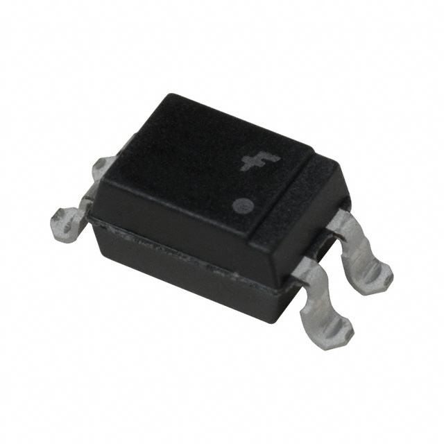
Product overview of the FOD814A3SD Optoisolator
The FOD814A3SD optoisolator represents a refined solution for applications requiring robust electrical isolation between logic-level control circuits and power-side switching elements. At its core, the device leverages a gallium arsenide infrared emitting diode optically coupled to a silicon phototransistor, maintaining physical separation between the input and output paths. This architecture not only suppresses conducted and radiated transients but also ensures signal integrity amid substantial potential differences—facilitating up to 5,000 VRMS withstand voltage across the isolation barrier without significant signal degradation.
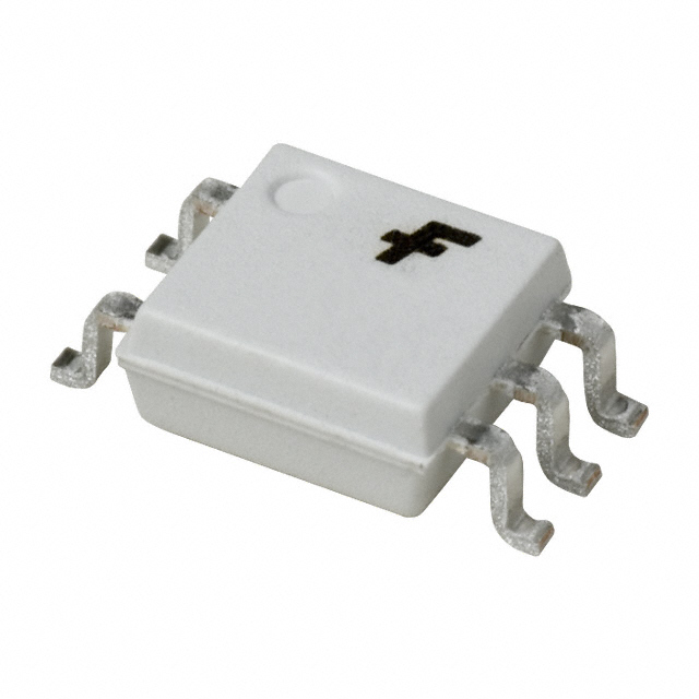
Integration into compact designs is achieved by the 4-SMD gull-wing package, addressing high-density PCBs typical in industrial automation and measurement modules. The package’s small footprint streamlines board layout and facilitates automated assembly processes. Its surface-mount configuration also enhances thermal management and mechanical reliability in environments prone to vibration or thermal cycling.
Electrical parameters such as CTR (current transfer ratio) stability across wide temperature ranges and minimal propagation delay are fundamental for precise signal transmission. These attributes make the device particularly effective in feedback circuits for switch-mode power supplies, communication interfaces between microcontrollers and high-voltage domains, and line receivers in programmable logic controllers. The optoisolator sustains performance in environments subjected to electrical noise, ensuring reliable state transitions and minimizing the risk of latch-up or data corruption—a common issue in mixed-signal systems.
The device’s compliance with ROHS3 and REACH not only simplifies design certification but also future-proofs the component against regulatory shifts in hazardous material content. Its MSL 1 rating directly supports flexible logistic and manufacturing strategies, as unrestricted floor-life streamlines material handling during production runs. This is essential in contract manufacturing and field-repair scenarios, where unanticipated delays or extended storage are typical.
In practical scenarios, implementation best practices involve optimizing the external resistor values to guarantee sufficient LED drive current, accounting for expected worst-case CTR. Proper PCB layout techniques—such as maintaining generous creepage and clearance distances and minimizing parallel traces across the isolation barrier—further enhance system resilience. Implementing these measures consistently yields reliable performance across a product’s lifetime, even when subjected to erratic transients or repetitive surges.
A major insight in isolation system design is that device reliability extends beyond compliance figures—it lies in anticipating and mitigating edge-case failures, particularly in brownfield upgrades or retrofit scenarios where legacy systems impose unanticipated stressors. Selecting FOD814A3SD as the isolation element brings not only standard-compliant specification but a practical balance of electrical robustness, operational stability, and design flexibility that directly translates into extended system uptime and simplified engineering workflows.
Key functional principles of FOD814A3SD
The operational methodology of the FOD814A3SD centers on dual gallium arsenide infrared LEDs arranged in inverse parallel, providing inherent bidirectional sensitivity. This configuration is crucial for AC waveform compatibility, facilitating responsive detection regardless of input polarity. As the input signal is applied, the corresponding LED conducts based on the signal’s phase, modulating light transmission toward the silicon phototransistor. The phototransistor, engineered for rapid switching and consistent current transfer ratio, interprets the optical signals, yielding a distinct and isolated electrical output.
The core optoisolation mechanism eliminates electrical continuity between the input and output domains. This separation not only safeguards sensitive downstream circuitry but also suppresses ground loops and transient interference common in high-voltage environments. In practical deployment, such as power-line monitoring or telecommunication interfaces, the device reliably relays small control signals across disparate system potentials. Continuous operation under variable input conditions demonstrates the robustness of gallium arsenide emitters and their stable luminous efficacy, with negligible degradation in harsh electrical surroundings.
Design decisions, such as selecting dual inverse-parallel emitters, reflect a nuanced approach to ensuring seamless operation across both DC and AC regimes, with automatic adaptation to signal polarity. Field implementations reveal that input surges or indeterminate line voltages do not compromise the isolation barrier; the phototransistor maintains fidelity, ensuring that output signals mirror true input states without inadvertent triggering or signal distortion.
Advanced system architects can leverage the FOD814A3SD’s architecture for low-level logic interfacing where reliable isolation is mandatory, particularly in mixed-signal environments where digital controllers interact with high-voltage domains. The layered optoelectronic construction ensures not only basic isolation but also robustness against electrical noise and transients, with minimal propagation delay. These design features position the device as an optimal choice for industrial control systems demanding both safety and signal integrity, making it a versatile component within isolation-critical signal pathways.
Electrical characteristics of FOD814A3SD
The electrical characteristics of the FOD814A3SD are governed by a careful balance between input drive requirements, transfer efficiency, output dynamic range, and isolation robustness, making it suitable for demanding signal isolation and interface applications.
Examining the input parameters, the forward voltage threshold—typically 1.2 V at 20 mA—ensures compatibility with standard logic levels, while limiting power dissipation on the input side. A maximum of 1.4 V provides sufficient design margin, accommodating fluctuations within input drive circuitry. This precise specification streamlines current-limiting resistor selection and enables straightforward interfacing with microcontrollers and digital output stages.
Current transfer ratio (CTR) represents the device’s optoelectronic conversion efficiency. The FOD814A3SD offers a CTR window of 50–150% at 1 mA input and 5 V collector-emitter voltage. This broad range simplifies circuit tolerance management and allows for consistent switching performance across manufacturing and temperature variations. However, for applications where stable CTR is critical—such as analog signal transmission or precision feedback circuits—careful calibration and bin selection may be practiced to mitigate the impact of CTR drift over device lifetime or ambient shifts. In practice, operating near the median value within this CTR band tends to achieve optimal reproducibility and signal linearity, especially when scaling designs for mass production.
The output stage supports a peak collector current of 50 mA, significantly extending load-driving capability, while a collector-emitter breakdown voltage of 70 V means the device accommodates moderate-level switching and interfacing requirements in industrial control architectures. The 6 V emitter-collector breakdown constraint influences reverse-bias handling and must be acknowledged during transient or reverse-polarity scenarios. Application experience underscores the importance of observing derating curves, particularly in mixed-voltage systems, ensuring that neither output current nor VCEO thresholds are stressed under fault conditions or during startup transients.
Switching dynamics, marked by a rise time of 4 μs and fall time of 3 μs, translate into mid-frequency response, which aligns with signal isolation for analog or digital communication up to 80 kHz (-3 dB bandwidth). This performance proves reliable in environments where moderate-speed control signals, PWM feedback, or sensor interfaces are present. The interplay between input drive—often maintained at 20 mA for rapid response—and load resistor selection (typically 100 Ω–1 kΩ) offers flexibility in tailoring risetime/fall-time tradeoffs, allowing optimization for edge sharpness versus power consumption. In real-world scenarios, minimizing output load capacitance and avoiding extraneous wiring length can further enhance response fidelity.
Low collector-emitter saturation voltage, below 0.2 V (at 1 mA output and 20 mA input), minimizes output voltage drop and heat generation, supporting efficient low-loss switching. This trait is particularly valued in designs with tightly regulated power supplies, where minimizing the impact of component-level voltage drops contributes directly to overall system stability and energy efficiency.
The isolation barrier’s quality is evidenced by insulation resistance exceeding 10¹¹ Ω at 500 V and a low input-output capacitance of 0.6–1.0 pF. This high resistance and capacitive isolation ensure negligible leakage and superior common-mode transient immunity, reinforcing signal integrity even in electrically hostile environments. In practice, such devices are routinely deployed in power supply feedback, signal monitoring, and ground loop elimination contexts, where electrical isolation is indispensable for functional safety and data reliability.
Thermal operating range, extending from –55°C to +105°C, underscores the component's durability in both extreme industrial installations and tightly constrained enclosures. The ability to maintain signal fidelity and switching consistency across this spectrum is achieved through meticulous device architecture and material selection. Experience suggests that designs capitalizing on the FOD814A3SD’s extended temperature range exhibit reduced failure rates in surge-prone or thermally unstable platforms, favoring long-term operational robustness.
Ultimately, the FOD814A3SD’s electrical profile reflects a design philosophy that values versatility and intrinsic safety. Its parameter set directly addresses the needs of control systems, precision interfaces, and power-constrained environments, enabling scalable, reliable isolation without overengineering complexity or cost. The interplay among CTR range, switching speed, and insulation barrier character is central to selecting appropriate optocouplers in systems demanding balanced electrical performance and high-integrity isolation.
Thermal and mechanical specifications of FOD814A3SD
Thermal and mechanical performance parameters of the FOD814A3SD are foundational for robust component integration within compact electronic assemblies. The device sustains an absolute maximum power dissipation of 200 mW overall, with a separate allocation of up to 150 mW for its detector segment. These thresholds ensure reliable operation even under sustained switching or elevated ambient temperatures, provided designers implement appropriate derating in thermally dense systems. Device longevity and stability link closely to the specified junction-to-case thermal resistance of 210°C/W; this value defines the efficiency of thermal transfer from the internal junction to the case surface. Integrating adequate thermal vias and copper pours directly beneath the device footprint on the PCB optimizes heat dissipation, preventing localized hot spots that could drive junction temperatures beyond safe limits.
Soldering process tolerances are precisely defined to accommodate high-throughput automated reflow methods. The FOD814A3SD’s leads withstand soldering temperatures of 260°C for up to 10 seconds, aligning with industry-standard reflow profiles. Peak package temperatures are not to exceed 260°C, enforced by recommended ramp rates below 3°C/s during heat-up and below 6°C/s for cooldown, with the total thermal excursion limited to eight minutes per cycle. Adhering to these thermal envelopes prevents package delamination and maintains internal insulation integrity. Manufacturing experience suggests employing thermal profiling in mass production as subtle variations in equipment can produce transient peaks; high-mass boards and densely populated layouts benefit from careful thermal chamber calibration to avoid overstress.
Mechanically, the 4-pin surface-mount device with gull wing leads facilitates standard pick-and-place operations. The package footprint is optimized for PCB density while still offering substantial creepage and clearance: an external minimum of 7 mm is maintained, ensuring robust isolation even in high-potential difference environments. An insulation thickness ≥0.4 mm delivers additional safety margins, enabling the FOD814A3SD to satisfy stringent regulatory conditions for reinforced insulation in industrial and medical applications.
Layered design approaches benefit from viewing the FOD814A3SD not just as an isolated component but as an enabler of system-level insulation and reliability. In high-isolation signal chains—such as gate drives for power electronics or signal interfaces crossing hazardous voltage domains—the specified mechanical spacings and thermal characteristics permit tighter integration without sacrificing safety. Notably, the gull wing package’s proven compatibility with both conventional solder pastes and lead-free processes streamlines bill-of-materials standardization across product lines.
A deeper review of device implementation underscores the importance of holistic thermal management and mechanical planning. Even with strong standalone characteristics, the broader assembly context—encompassing PCB layer stack-up, airflow, and proximity to heat-generating neighbors—exerts a significant influence on operating margins. Optimal application of the FOD814A3SD leverages its high-reliability design limits, ensuring both safety compliance and sustained field performance in mission-critical or extended service environments.
Safety, compliance, and insulation performance of FOD814A3SD
Safety and insulation performance parameters of the FOD814A3SD are primarily defined by its robust optocoupler architecture, where a high-performance optical isolation barrier underpins the device’s core functional platform. Certification to UL1577 and DIN EN/IEC60747-5-5 is not only declarative but results from stringent dielectric testing, ensuring a verified input-to-output isolation voltage up to 5,000 VRMS for one minute. This high isolation rating directly supports compliance in installations categorized under less than 150 VRMS and 300 VRMS (DIN VDE 0110/1.89), reflecting alignment with typical requirements for reinforcing insulation in industrial automation, precision instrumentation, and grid interface designs.
The insulation system extends its reliability through a Comparative Tracking Index (CTI) of 175, which denotes the device’s strong resistance to surface discharge phenomena under the influence of contaminating agents—essential in environments where conductive dust or chemical vapors may be present. The Pollution Degree 2 classification further points to suitability in control cabinets and power conversion circuits, where only non-conductive pollution normally occurs and condensation is unlikely, but transient failures could have outsized operational impacts.
Thermal endurance is another critical layer influencing deployment decisions. The package is engineered to withstand transient case temperatures up to 175°C. However, safety limit ratings mandate external protective circuitry such as thermal shutdown circuits, fusing, or redundant monitoring to guarantee system-level reliability under single-fault or abnormal thermal runaway events. This positioning allows for robust integration into high-power drives, inverter systems, and feedback control paths, where occasional high-junction temperatures are anticipated due to fault surges or overload transients.
Transient over-voltage withstand capability (VIOTM) up to 8,000 V provides confidence for designers facing margin stacking requirements dictated by insulation coordination standards. With appropriate PCB layout techniques—such as maximizing creepage and clearance distances—system integrators can capitalize on the FOD814A3SD’s full insulation envelope without external derating. This capability is particularly leveraged in scenarios where insulation failure is not an option, such as medical diagnostic equipment, grid-coupled power electronics, or industrial robotics.
Practical experience reveals that stable performance and long-term reliability are best attained when the insulation characteristics are complemented by deliberate derating and real-time monitoring. For instance, periodic verification of barrier integrity using in-system dielectric strength testing, and careful management of local hotspots around the isolation package, help ensure durability far beyond minimum datasheet specifications. Notably, the strong safety and compliance posture of the FOD814A3SD is fully realized only when installation best practices—like routing sensitive signals away from high-voltage planes and rigorous PCB cleanliness control—are meticulously observed.
Considering evolving application requirements, the architecture of the FOD814A3SD suggests further potential for functional integration and predictive diagnostics, enabling engineers to more precisely track isolation degradation mechanisms in real time. This anticipatory approach is becoming increasingly vital in safety-critical sectors, accentuating the strategic advantage of devices that exceed only-the-minimum compliance and offer comprehensive insulation assurance.
Application scenarios for FOD814A3SD
The FOD814A3SD optoisolator demonstrates robust versatility as a solution for diverse signal isolation challenges across advanced electrical systems. At its core, the device leverages phototransistor output and optimized coupling efficiency, resulting in high common-mode transient immunity (CMTI) and reinforced galvanic isolation. This architecture directly addresses noise immunity and safety requirements, especially when system nodes must be protected from high-potential transients or unpredictable line voltages.
Within AC line monitoring circuits and DC polarity sensing applications, the FOD814A3SD excels due to its bidirectional input compatibility. It reliably detects both AC and varying-polarity DC signals, even under the stress of floating grounds or line disturbances. Its high isolation voltage ensures that low-voltage measurement or control subsystems remain unaffected by line surges or faults, a property further supported by stable current transfer ratio (CTR) groupings. In practical circuit integration, careful selection of input resistors and attention to CTR binning can optimize threshold detection while minimizing drift over temperature and time.
In industrial automation and telecommunications interfaces, the separation of control and power domains benefits from the FOD814A3SD’s reliable barrier. Complex environments often present unpredictable surges, switching transients, and electromagnetic interference. The optoisolator’s fast switching characteristics, combined with its suitably low input drive current requirements, allow seamless buffering of digital inputs from programmable logic controllers (PLCs), sensor lines, or remote communication links. Empirical field observations confirm that employing the FOD814A3SD minimizes vulnerability to noise-induced misoperation, especially in dense signal routing scenarios.
The device finds critical application in telephone line isolation circuitry. Its capability to filter hazardous voltages, suppress transients, and eliminate ground loops directly translates to improved call quality and extended system lifespan. For legacy exchanges being upgraded to signal processors or IP telephony hardware, retrofitting with FOD814A3SD-based isolation has proven effective for both electrical safety and operational continuity.
Microprocessor input isolation, digital logic buffering, and interface protection further illustrate the component’s practical advantage. When used at the digital front end, the optoisolator shields sensitive microcontroller units (MCUs) from asynchronous spikes and external faults. Its robust switching response—when tuned with respect to load capacitance and layout—supports high-frequency digital environments without introducing critical propagation delays. It is essential, however, to address load conditions and ensure that the thermal environment stays within the manufacturer’s recommended envelope, as excessive dissipation can impact long-term CTR stability.
A nuanced aspect often overlooked is the significance of matching CTR grades to specific signal integrity requirements. Over-conservative selection may result in excess input drive and reduced efficiency, while under-specifying invites unreliable operation under marginal conditions. Experience suggests that balancing switching speed and CTR consistency results in a more resilient and predictable design, especially when scaling up to system-wide deployments or modular architectures. Integrators often find that starting with the device’s median CTR bin, then performing parametric tuning based on board-level characterization, delivers the most robust outcomes.
The FOD814A3SD thus serves as more than a basic isolation barrier; it is a precision-engineered component whose full potential emerges when subtle electrical, thermal, and system-level considerations are interwoven into the deployment strategy. The interplay between device parameters and application context ultimately defines the reliability and survivability of both legacy and next-generation electronic systems.
Potential equivalent/replacement models for FOD814A3SD
Evaluating equivalent or replacement options for the FOD814A3SD necessitates a precise examination of electrical characteristics, package compatibility, and long-term supply chain robustness. Within the onsemi portfolio, the FOD817 series emerges as a primary candidate, engineered with a high isolation voltage rating of 5,000 VRMS and utilizing a silicon phototransistor output. This series differentiates itself through multiple sub-models (FOD817A through FOD817D), each tuned with distinct Current Transfer Ratio (CTR) groups spanning 50% to 600%. This granularity in CTR selection enables fine adjustment of signal sensitivity and output drive, allowing adaptation to a range of phototransistor interfacing scenarios, particularly in circuits where logic level translation integrity is critical.
The FOD814 standard variant extends the available CTR window to 20–300%. This broader range supports applications demanding controlled optocoupler sensitivity, especially when interfacing with slower logic or where wider signal margin is permissible. When scrutinizing input side configurations, differences in LED forward voltage and recommended input current thresholds emerge. Variations here influence system-side LED drive design, hold significance for input current headroom, and dictate compatibility with the intended control circuitry.
Packaging considerations play a direct role in production yield and field reliability. Both the FOD814 and FOD817 series cover standard DIP and SMD profiles, with lead spacing variants that accommodate diverse PCB designs—from high-voltage isolation tracks to densified layouts where PCB real estate is limited. Model choice frequently hinges on assembly workflow—automated pick-and-place lines may benefit from SMD options, while traditional through-hole designs leverage DIP formats for strong mechanical anchoring.
Real-world deployment frequently uncovers nuances not always evident from datasheets. For example, manufacturing test yields can be influenced by the consistency of CTR across production batches; tighter CTR distributions in some FOD817 sub-models enhance predictability in performance-critical designs. Environmental performance under humidity and temperature extremes further distinguishes models—lead finish, encapsulant robustness, and package dimensions intersect with end-system reliability demands.
A layered selection approach proves advantageous. Starting with primary electrical parameters (CTR, isolation, forward voltage), integrating package/assembly constraints, and then validating against practical reliability metrics in the application context, minimizes unforeseen failure modes. Notably, second-sourcing strategies benefit from dual-vendor qualification using standard footprint and CTR groupings, streamlining BOM interchange and mitigating supply risk.
Optimal substitution thus derives from a holistic understanding of both signal chain intricacies and the mechanical-electrical interface with the host system. Attention to subtle parameters—such as CTR drift over aging, LED transfer efficiency, and encapsulant optical integrity—differentiates robust design from merely compatible replacement. This systems-level perspective enhances procurement agility while safeguarding operational margin in mass production.
Conclusion
The onsemi FOD814A3SD optoisolator is engineered for high-integrity electrical isolation, leveraging an optimized internal structure that reliably separates input and output domains to prevent the transmission of unwanted transients or ground loops. The device’s fast switching capabilities—achieved through precise emitter-receiver alignment and low propagation delay—enable efficient signal processing in circuits requiring accurate timing and minimal interference, such as industrial process controllers and measurement systems. The selectable current transfer ratio (CTR) affords granular control, allowing designers to tailor input-output response according to specific load and sensitivity requirements. This parameter flexibility is particularly beneficial for feedback interfaces and digital communication protocols, where signal fidelity and bandwidth are critical.
Electrical performance is safeguarded by a rigorous adherence to safety and industrial standards, including compliance with reinforced isolation ratings and international certifications. The robust insulation material and compact SMD packaging balance space constraints typical of dense PCB layouts with reliable long-term operation—favoring automated assembly processes and high-volume manufacturing. The device can accommodate broad input voltage ranges, further expanding compatibility with diverse sensor interfaces, microcontroller outputs, and programmable logic devices.
Integration considerations should start with accurate characterization of CTR tolerance, input currents, and maximum collector-emitter voltages, closely matched to application-specific requirements. Thermal management is crucial for maintaining optimal CTR across elevated ambient temperatures and minimizing performance drift over device lifetime. In high-reliability scenarios, optimal spacing and creepage/clearance planning around the optoisolator footprint enhance operational safety and conformity to local regulatory codes.
From practical deployment experience, leveraging the FOD814A3SD in isolation stages between noisy power switching environments and precision analog domains markedly improves signal integrity. In safety-critical embedded systems, its consistent CTR behavior under variable supply conditions ensures dependable logic-state transmission, directly impacting uptime and maintenance cycles. Subtle differences in pinout or transfer characteristics among alternative onsemi models allow for seamless second-sourcing and future hardware revisions, maintaining both supply chain stability and platform compatibility.
The combination of robust isolation, high-speed switching, and parametric versatility positions the FOD814A3SD as a core component for scalable measurement and control architectures. Its design resilience, fortified by rigorous validation and available form factor options, helps realize fault-tolerant systems that demand uncompromising signal isolation, especially when long-term operational reliability and regulatory adherence are non-negotiable. This approach to optoisolator selection centers on aligning device strengths with practical application requirements, facilitating engineering-driven advancements in modern industrial electronics.