>
>


Product overview for Nexperia PMV100EPAR P-Channel Trench MOSFET
The PMV100EPAR leverages advanced Trench MOSFET architecture, enabling low on-state resistance with minimal gate charge. This design fundamentally improves switching speed and reduces conduction losses, which are crucial in modern power management units where both efficiency and thermal behavior govern system reliability. The P-channel enhancement mode characteristic simplifies high-side and load switching, removing the need for complex gate drive arrangements that would otherwise increase component count and reduce board-level efficiency. Operating with a gate threshold voltage engineered for direct logic-level compatibility, the device integrates seamlessly with microcontroller outputs and other digital logic domains, streamlining control circuitry on mixed-voltage boards.
Thermal management is a key consideration in compact electronic systems, and the PMV100EPAR addresses this by supporting robust continuous drain current handling at elevated temperatures, owing to its silicon process optimizations and minimized package thermal impedance. In practice, the SOT-23 form factor emerges as an optimal solution for densely populated layouts, particularly in automotive ECUs, notebook DC-DC converters, and battery-powered IoT modules. Engineers exploiting automated assembly benefit from the consistent solderability and mechanical reliability, allowing for scalable surface-mount production with high process yields.
From the layout standpoint, consideration of current paths and careful via placement adjacent to the source lead yields noticeably reduced hotspot formation on PCBs, leading to extended operating lifetimes, especially in ambient conditions typically exceeding 60°C. Real-world deployment illustrates that the device maintains switching integrity at fast edge rates, minimizing voltage overshoot thanks to controlled gate charge and intrinsic capacitance levels tailored through the trench process geometry. This performance stability supports various fault-tolerant topologies, such as reverse polarity protection and load disconnect circuits where consistent turn-off behavior under transient events is imperative.
Employing PMV100EPAR in systems sensitive to electromagnetic interference often results in lower radiated emissions due to optimized switching slopes and reduced parasitic inductance associated with its leadframe and die configuration. Application in renewable energy conversion, automotive body electronics, and high-frequency power supply modules demonstrates how trench P-channel MOSFETs bridge the gap between stringent size constraints, demanding efficiency targets, and board design agility. The PMV100EPAR stands as a representative solution for designers who prioritize integration, switching performance, and reliability within next-generation, space-optimized platforms.
Key features and technical highlights of Nexperia PMV100EPAR
The Nexperia PMV100EPAR integrates advanced trench MOSFET technology, enabling a very low on-resistance profile. The typical RDS(on) of 100 mΩ at VGS = -10 V with ID = -2.2 A directly contributes to minimized conduction losses, especially in power-sensitive applications. This low-resistance characteristic stems from deep trench structures that enhance carrier mobility and reduce channel bottlenecks, optimizing current flow and thermal performance. As a result, designers can deploy this MOSFET in demanding switching and load control environments where energy efficiency and heat management are paramount.
The device's logic-level gate drive, characterized by a gate threshold voltage spanning -1.9 V to -3.2 V, allows seamless interfacing with low-voltage microcontrollers and digital ICs. The drive requirements are reduced, enabling simplified external gate circuitry and eliminating the need for level shifters. This compatibility streamlines integration into embedded system boards, particularly in scenarios where gate voltage rails are tightly managed or where board space and part count must be minimized.
Built for resilience, the PMV100EPAR supports a junction temperature of up to 175°C, which extends operational reliability and safety margins in harsh automotive and industrial conditions. This wide temperature tolerance is engineered through optimized silicon and packaging processes, ensuring consistent electrical characteristics under thermal stress. Field deployments in engine compartments, motor drives, and industrial robotics benefit from such robustness, maintaining functional integrity over prolonged duty cycles and fluctuating ambient conditions.
AEC-Q101 qualification anchors the PMV100EPAR’s credibility for deployment in automotive-grade scenarios. The qualification process encompasses rigorous stress screening for reliability and failure mode mitigation, providing assurance against common application hazards such as thermal cycling, humidity, and voltage transients. Regulatory compliance not only expedites design approval but also reduces warranty and lifecycle risks in vehicular control units and safety-critical subsystems.
Switching performance is sharpened by a low total gate charge of 17 nC and an input capacitance of 616 pF. Such parameters facilitate rapid charge/discharge cycles at the gate, enabling high-frequency switching without excessive drive current. This is advantageous in DC-DC converter topologies, motor control circuits, and rapid load switching environments where switching efficiency directly translates to reduced EMI and superior overall system response.
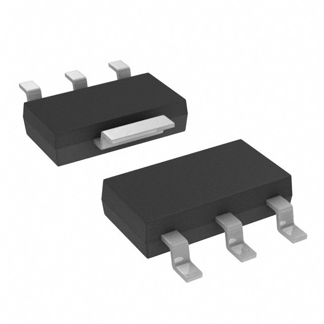
From a layout and form-factor perspective, the SOT-23 package dimensions (2.9 mm × 1.3 mm × 1 mm) with a 1.9 mm pin pitch offer significant PCB space savings. This compact footprint provides engineers latitude for dense component placement, supporting miniaturized designs and complex multi-channel power management architectures. Practical deployment tends to leverage the package’s thermal and electrical characteristics by pairing with optimized copper area and low-inductance routing, reducing both parasitic losses and heat build-up.
A distinctive strength of this MOSFET lies in its balanced profile—offering not only energy and thermal efficiency but also robust EMC performance by virtue of its fast switching traits and stable gate drive behavior. Application scenarios encompassing automotive sensor regulators, industrial automation modules, and portable power stages benefit from reduced design complexity, improved reliability margins, and scalable integration—characteristics that elevate engineering productivity and accelerate product time-to-market.
Performance characteristics and operational parameters of Nexperia PMV100EPAR
The Nexperia PMV100EPAR exhibits a well-balanced set of electrical and thermal characteristics, enabling precise integration into compact power management and switching circuits. Its drain-source breakdown voltage of -60 V offers a dependable margin for designs subjected to moderate supply transients, making the device suitable for applications in protected power rails, signal line switching, and low-side load drivers where negative voltages may be encountered. The continuous drain current rating of -2.2 A at 25°C, decreasing to -1.4 A at 100°C, reflects well-managed thermal behavior—especially relevant for densely packed designs where junction temperature control is critical. Momentary demands for higher current, up to 6 A in short pulses (≤10 μs), allow for effective handling of load surges or inrush events, provided that PCB copper thickness and layout minimize parasitic inductance.
Gate-source voltage tolerance, spanning ±20 V, enables flexibility in gate drive strategies. This accommodates both direct microcontroller outputs as well as dedicated gate drivers, reducing risks posed by accidental voltage overshoots or noise coupling in mixed-signal environments. The internal structure supports avalanche energy absorption of up to 33 mJ, an essential safeguard against voltage spikes encountered during inductive load switching. This translates to lower external protection component counts and facilitates streamlined layouts for relay emulation, solenoid drivers, or flyback converter control.
Thermal management is a defining consideration for maximizing the PMV100EPAR’s performance envelope. Power dissipation is rated at 710 mW on standard FR4 at 25°C, escalating to 8.3 W when optimal solder-point heatsinking is applied. Real-world board layouts exploit wide copper planes beneath the source pads and minimal thermal resistance via thick traces, supporting efficient power transfer while minimizing temperature rise. During iterative design cycles, refined PCB topologies (including contiguous ground pours) effectively lower device operating temperature, achieving higher sustained currents without violating RDS(on) limits.
Dynamic response is accelerated by turn-on and rise times as brief as 7 ns, with turn-off and fall times of 29 ns and 25 ns, respectively. These characteristics facilitate high-frequency operation in switching regulators and logic-level translation, with fine-tuning possible via external gate resistance selection. Stable, low leakage—drain-source at -1 μA, and gate-source at ±100 nA—ensures negligible off-state losses, directly contributing to system idle power targets and safeguarding against leakage-induced signal corruption.
The temperature dependence of RDS(on) and gate threshold voltage demands consideration during design and validation. On-state resistance climbing to 276 mΩ at 175°C highlights the necessity for accurate derating and margining; systems built for sustained high current must incorporate conservative thermal modeling, exploiting advanced PCB heatspreading or additional airflow to avoid electrical overstress. Under reduced gate drive (VGS = -4.5 V), the increase in RDS(on) must be weighed against drive IC capabilities, especially in cost-sensitive or battery-powered designs. Balanced trade-offs between turn-on speed, EMI containment, and drive voltage are achieved through empirical gate resistor selection—best results often stem from iterative bench testing and waveform analysis.
Robust ESD capability, with HBM withstand up to 400 V, provides reliability in manufacturing and end-use environments subject to routine handling. Layout strategies minimizing gate trace lengths and comprehensive component placement reduce system-level risks, while device-level protection facilitates compliance with consumer and industrial robustness standards.
In deploying the PMV100EPAR, circuit designers leveraging its fast switching, low leakage, and strong avalanche ratings can enable compact, efficient solutions with superior transient immunity. The interplay of electrical parameters and thermal behavior is complex; careful attention to PCB design, switching profiles, and gate drive sources is imperative for unlocking the full performance bandwidth. With its broad voltage and current operating ranges and reliable ESD protection, the PMV100EPAR’s practical versatility is enhanced when nuanced design techniques and real-world validation are systematically integrated into the development workflow.
Thermal management and reliability for Nexperia PMV100EPAR
Thermal management strategies for the Nexperia PMV100EPAR are fundamental to its operational reliability, especially in power-dense or temperature-critical contexts. At the base level, the device’s junction-to-ambient thermal resistance ranges from 175 to 210 K/W under free-air conditions with a standard PCB footprint. This intrinsic parameter immediately underscores the pivotal role of board architecture in overall heat dissipation; actual thermal performance is not dictated solely by the transistor, but critically by the surrounding system design.
Optimal results are achieved through targeted PCB engineering. Increasing copper area, deploying thermal vias beneath the device, and employing multi-layer ground planes can bring junction-to-solder point thermal resistance down to the 13–18 K/W range. This dramatic reduction directly impacts allowable steady-state and transient loads, permitting the PMV100EPAR to handle higher power throughput without exceeding maximum junction temperature. The device’s specification for sustained junction and ambient operation up to 175°C offers latitude for deployment in environments subject to peak thermal excursions—such as engine bays, industrial control cabinets, and compact sealed systems—when thermal paths are carefully constructed.
Thermal impedance curves and standardized derating characteristics offer designers quantitative tools for precise heat-flow modeling. Time-dependent scenarios, including periodic load spikes or variable ambient conditions, can be mapped using provided thermal impedance data, facilitating lifecycle analysis and preemptive mitigation of thermal runaway risks. Derating curves, in particular, inform safe operating area boundaries and help avoid over-design or unnecessary margin, enabling more compact designs without sacrificing reliability.
Further, the device’s compliance with AEC-Q101 reflects robust screening and qualification for automotive reliability requirements. This certification is not merely nominal; it translates to predictable behavior under vibration, humidity, and temperature cycling—conditions typical in mission-critical mobile electronics and harsh industrial domains. Experience in implementing similar automotive-grade MOSFETs indicates that failure rates and thermally-induced degradation can be sharply reduced by combining conservative component selections with aggressive PCB thermal routing, yielding systems that maintain tight electrical tolerances in demanding, enclosed modules.
Integrated analysis reveals that leveraging PMV100EPAR’s full performance envelope requires simultaneous attention to both component-level data and holistic thermal design. Examining datasheet graphs in context of real-world PCB stack-ups and airflow regimes reveals otherwise hidden headroom for power scaling and helps prevent thermal derating bottlenecks. For advanced scenarios, active cooling, dynamic load balancing, and thermal feedback loops can be introduced if passive methods prove insufficient, ensuring sustained functionality well inside the device’s published temperature limits.
Ultimately, mastery of thermal management for PMV100EPAR hinges on translating specification-level data into tangible board-level outcomes. The ability to predict, measure, and iterate on thermal performance—using not only datasheet parameters but also simulation and empirical board characterization—forms the basis for exceeding reliability standards in high-power, high-density applications. Carefully engineered thermal solutions unlock the full potential of automotive-grade MOSFETs, yielding platforms where robust operation and minimal maintenance are sustained across extended service intervals.
Application scenarios for Nexperia PMV100EPAR in modern electronics
The PMV100EPAR, a Nexperia logic-level MOSFET, leverages key physical characteristics—fast switching speed, notably low RDS(on), and a compact SOT23 surface-mount footprint—to address pressing design requirements in modern electronics. Its intrinsic low channel resistance ensures efficient current conduction and minimal power loss, critical for systems where voltage overhead is tightly budgeted. The device's switching response enables precise control over transient events, reducing electromagnetic interference and allowing for finer timing margins in synchronous designs.
At the circuit level, the PMV100EPAR excels as a high-side load switch on DC power rails, optimizing both thermal dissipation and voltage stability. Implementation in supply switching reveals the advantage of low gate charge, which allows direct interface with microcontroller GPIOs and minimizes propagation delays. Analysis of load switching tests confirms this MOSFET’s suitability where rapid on/off cycling and current surges challenge legacy designs. Its form factor further alleviates layout density restrictions, streamlining PCB routing for portable and space-critical assemblies.
In relay driver circuits, the PMV100EPAR supports both electromechanical and SSR applications by reliably delivering actuation current at logic-level gate potentials. This unity between control logic and power devices simplifies cross-domain integration, reducing the need for intermediate level-shifting and facilitating embedded automation. Empirical validation demonstrates consistent turn-on behavior and robust thermal handling under pulse conditions typical in relay operation. These attributes contribute to longer relay life cycles and stable field performance.
The MOSFET’s high-speed switching capacity also enhances bandwidth in line driver and signal switching topologies for communication interfaces. Deployment in data acquisition or bus isolation modules capitalizes on sub-microsecond edge rates, mitigating crosstalk and simplifying compliance with signal integrity budgets. Its repeatable performance under load transients and noise conditions supports reliability in industrial networks, where deterministic operation is paramount.
General power switching across consumer, industrial, and automotive domains is enabled by the PMV100EPAR’s balance of power density and operational flexibility. Integration in motor drives, battery management, and regulated power modules demonstrates that thermal behavior remains predictable, even under elevated ambient temperatures. The device's qualification to automotive-grade standards expands deployment possibilities to mission-critical areas such as engine control, advanced driver-assistance systems, and in-vehicle infotainment architectures. Extended temperature tolerance and ESD robustness ensure resilience in harsh operating environments.
Unique circuit behaviors emerge when combining the PMV100EPAR’s low RDS(on) and fast switching with advanced board-level design techniques. Parallel orientation in multi-switch arrays can scale current capacity without significant layout penalty; switching synchronization can suppress voltage overshoot and minimize radiated EMI. These accrued effects reinforce the MOSFET’s position not merely as a functional element, but as a cornerstone of compact, energy-efficient electronic design, thriving at the intersection of speed, integration, and reliability.
Potential equivalent/replacement models to Nexperia PMV100EPAR
Selecting suitable equivalents or replacements for the Nexperia PMV100EPAR involves careful examination of the underlying Trench MOSFET structure and its influence on core device parameters. The PMV100EPAR’s specific value lies in its synergy of low RDS(on), moderate gate charge, and compact SOT-23 footprint, which together define its efficacy in power switching and load management circuits.
When exploring alternatives, such as Nexperia’s own PMV100EPA variant or P-channel Trench MOSFETs from manufacturers like Vishay (SI2333DS) and ON Semiconductor (FDN306P), emphasis must remain on aligning key performance metrics. Each candidate’s breakdown voltage and maximum current rating establish fundamental safety and power handling capability. Subtle differences in RDS(on)—especially measured at logic-level gate drive—directly affect efficiency and thermal performance. Engineers typically scrutinize gate charge profiles because these impact switching speed and, therefore, suitability in high-frequency applications or fast load transients. Footprint interchangeability, particularly the SOT-23/TO-236AB package, becomes essential, not only for PCB design reuse but also for minimizing requalification cycles in volume production.
Reliability parameters, including device qualification to automotive standards (such as AEC-Q101), process maturity, and long-term availability form a critical selection layer, particularly in regulated or mission-critical environments. Vendor consistency, historical field failure data, and roadmap stability significantly affect risk management throughout the product lifecycle. In practice, it is often observed that while datasheet parameters may match, variations in production lot stability or subtle packaging differences can manifest as yield drifts or assembly anomalies in high-reliability contexts.
Application scenarios further influence replacement strategy. In compact DC-DC converters, USB power switches, or battery protection circuits, slight deviations in threshold voltage or short-circuit robustness can impact both system functionality and downstream protection schemes. Experience indicates that, while modern Trench technology offers tight RDS(on) distributions, transient thermal and ruggedness behaviors still differ across ostensibly similar models.
Design optimization frequently hinges on nuanced trade-offs: lower RDS(on) may reduce conduction losses but could entail higher gate charge or limited surge current tolerance. Board-level thermal design and heat spreading must be recalibrated when switching vendors, given potential changes in package leadframe construction or internal bond wire layouts. Moreover, integrating alternative MOSFETs into designs often prompts additional system validation cycles, with a focus on pulse robustness and EMI emissions in actual end-use environments.
A refined approach leverages both electrical equivalency tables and empirical validation data, prioritizing sources with robust quality management and clear long-term support. This dual-pronged strategy addresses not only the functional interoperability between MOSFET variants but also the overarching supply chain and quality assurance dynamics essential for sustained product success.
Conclusion
The Nexperia PMV100EPAR P-Channel Trench MOSFET leverages advanced trench gate technology to optimize charge carrier flow, resulting in low specific on-resistance (Rds(on)) while maintaining a compact SOT-23 package footprint. This structural refinement enables efficient power switching under high-density board conditions, enhancing thermal dissipation and minimizing conduction losses—a pivotal attribute for applications with restricted layout space and stringent efficiency targets.
A critical design feature is its logic-level gate drive compatibility, which allows direct interfacing with low-voltage microcontrollers and digital logic circuits. This reduces the need for intermediate driver stages, streamlining system architecture and lowering overall BOM cost. The device's rapid switching capability, supported by minimized gate charge and optimized parasitics, translates to reduced switching losses and higher operational frequencies. This enables finer current regulation and improved transient response in power management circuits, particularly relevant in automotive ECUs and precision industrial controllers.
The PMV100EPAR's robust AEC-Q101 qualification certifies its resilience against automotive-grade stressors, such as wide temperature excursions, voltage surges, and repetitive thermal cycling. This level of qualification instills confidence in long-term reliability, even when deployed in critical path circuits for power distribution or load control. Extensive characterization data—ranging from safe operating area curves to avalanche energy ratings—further aids in derisking designs during the validation stage.
When selecting this device for circuit implementation, reference to key parameters such as maximum drain-source voltage, continuous current capacity, and Rds(on) behavior at various gate voltages is essential to ensure proper derating and prevent thermal runaway in field operation. Close examination of the SOT-23 thermal metrics can reveal potential margin improvements, for instance, via copper pour extensions or optimized PCB layout for enhanced heat sinking.
The PMV100EPAR is supported by comprehensive application notes and proven test results, allowing engineers to expedite design cycles through model-based simulation and hardware prototyping. For projects demanding equivalent or alternative devices, systematic cross-evaluation should weigh not only pin-for-pin compatibility and Rds(on) specifications, but also package thermal impedance, gate threshold voltage ranges, and long-term supplier stability. Such diligence can mitigate supply risk while maintaining system integrity.
In next-generation electronic platforms, the integration of the PMV100EPAR elevates power management strategies by enabling finer granularity in load switching, hot-plug control, and reverse battery protection. Its design synergy with modern power architectures underscores the momentum towards higher integration and smarter energy control. The device naturally aligns with the evolving priorities in automotive and industrial electronics—balancing miniaturization with uncompromised reliability and efficiency.