


 >
>


Product Overview: BZV55-C5V1 Good-Ark Semiconductor Zener Diode
The BZV55-C5V1 from Good-Ark Semiconductor is an SMD Zener diode optimized for compact voltage reference and stabilization circuits demanding reliable 5.1 V breakdown with efficient thermal characteristics. Leveraging the miniMELF (SOD-80) package, this device advances space-saving PCB layouts, making it particularly suitable for high-density board assemblies found in modern analog and mixed-signal modules. The 500 mW maximum power dissipation rating, coupled with a 5% Zener voltage tolerance, establishes a pragmatic balance between cost and parametric consistency.
At the device physics level, the BZV55-C5V1 employs a heavily doped p-n junction structure to realize sharp voltage clamping at 5.1 V within an operating current range that supports both precision biasing and general protection topologies. Its reverse breakdown mechanism is governed by the Zener effect, dominant at this voltage, yielding stable reference points even with fluctuations in supply rails. Practical deployment often utilizes the diode’s reverse-voltage-characteristic curve, allowing precise shunt regulation for low-current analog buffers, microcontroller supply rails, and critical sensor nodes.
Thermal management is integral due to the SMD miniMELF form factor’s limited heat sinking surface. Effective PCB trace design can mitigate junction temperature rise and sustain long-term reliability, especially under higher ambient conditions or surge loads. Layout optimization often involves maximizing copper under the device footprint and deploying local thermal vias to spread heat across multilayer stacks. Designers typically operate the diode at derated power levels below 400 mW when continuous regulation is required, ensuring drift and parametric shifts are minimized over product lifetime.
Within application circuits, the BZV55-C5V1 finds utility not only as a basic voltage reference but also as a robust clamp for overvoltage suppression in sensitive digital interfaces, where its fast transient response can prevent latch-up and data corruption. The 5% tolerance aligns well with environments where the reference voltage margin is less critical, such as auxiliary bias rails, LED drivers, and automotive sensor protection loops. In scenarios demanding tighter regulation, the device demonstrates low dynamic resistance, which, when incorporated with buffer transistors, supports cost-effective voltage reference cells.
Several design experiences highlight the importance of current limiting resistor selection, balancing between sufficient Zener knee current establishment and avoiding excessive steady-state dissipation. When deployed near its maximum power rating, periodic in-circuit monitoring has proven invaluable in detecting potential thermal overstress or solder fatigue in reflow environments. Additionally, leveraging this diode as a secondary line of defense in redundant protection schemes adds robustness, especially in portable and battery-operated systems where form factor and power budgets are constrained.
Overall, the BZV55-C5V1 exemplifies a device class where practical engineering trade-offs between mechanical miniaturization, electrical precision, and thermal robustness converge. By integrating the component within well-considered PCB designs and carefully curated operating envelopes, reliable voltage referencing and regulation can be achieved in a broad spectrum of high-density electronic platforms.
Key Features of BZV55-C5V1 Zener Diodes
The BZV55-C5V1 Zener diode leverages a silicon planar process to deliver uniform junction properties, which translates to consistent electrical behavior across temperature and operating ranges. Planar technology enables controlled breakdown voltage and low leakage currents, minimizing drift during extended operation and thermal cycling. The voltage grading, structured according to the E24 series, facilitates straightforward integration into international design platforms by offering granular increments, thus minimizing overdesign while meeting precise system requirements.
In the context of the BZV55-C5V1, the ±5% voltage tolerance targets robust yet cost-sensitive designs where ultra-tight regulation is nonessential. Tolerance delineation across the BZV55 series—extending to ±2% and ±3% options—provides a tunable tradeoff between precision performance and sourcing flexibility, particularly when the bill of materials must remain standardized across varying product lines.
Electrical engineers routinely deploy the BZV55 series as reference elements within shunt regulators, where its stable breakdown voltage supports reliable low-voltage stabilization under variable line and load conditions. In power management applications, these diodes absorb voltage transients and clamp overvoltage events, protecting downstream logic stages and analog interfaces. Their form factor and thermal behavior, deriving from the planar silicon construction, support high assembly densities on multilayer PCBs without exacerbating thermal hotspots—especially in scenarios where airflow or heatsinking is limited.
Utilizing the BZV55-C5V1 in microcontroller reset lines reveals its operational consistency when exposed to noisy supply rails or brown-out events, maintaining defined threshold levels that prevent microcontroller latch-up. Similarly, in analog sensor networks, the diode underpins signal conditioning blocks, holding reference nodes at stable potentials even as system headroom varies. Direct experience highlights the balance these diodes strike between cost efficiency and repeatability, particularly in large-volume production runs, where out-of-spec voltage references can propagate latent failures in the field.
A key insight lies in exploiting the broad E24 grading within the series—not only for voltage selection but to manage inventory complexity across modular boards. This strategy streamlines post-production calibration steps and increases supply chain flexibility, ultimately accelerating prototyping and reducing lead times. The underlying planar structure further reduces variability between lots, which is critical when designing for multi-sourced component footprints or when scaling system architectures horizontally across diverse market applications.
The BZV55-C5V1 thus embodies a blend of robust electrical fundamentals and pragmatic engineering tradeoffs, making it a preferred choice for baseline voltage regulation and general-purpose circuit protection where reliability, manufacturability, and ease of integration converge.
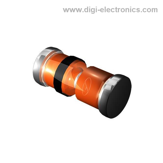
Mechanical Properties and Device Packaging of BZV55-C5V1
The mechanical properties of the BZV55-C5V1 are intrinsically tied to its encapsulation in the MiniMELF glass case (SOD-80), a configuration engineered for reliability within compact, densely populated electronic assemblies. The borosilicate glass enclosure delivers notable resistance to mechanical stresses encountered during automated assembly, reflow soldering, and on-field operation. This rigidity mitigates the risks of microcracks or physical deformation, ensuring stable electrical parameters across the device's operational life. The mass of approximately 0.05 g enhances PCB layout flexibility and facilitates precise component placement, reducing inertia during high-speed pick-and-place cycles and minimizing the likelihood of misalignment on high-density substrates.
Thermal cycling endurance is elevated by the glass encapsulation, which demonstrates low coefficients of thermal expansion matched closely with the silicon die. This synergy dampens thermomechanical stress at the die-package interface, a common failure point during repeated power cycling or environmental temperature shifts. Empirical deployment in reflow profiles confirms negligible drift in zener voltage and minimal delamination rates, supporting long-term stability in automotive and industrial contexts where temperature excursions are routine.
Device marking via the blue cathode band is optimized for both human factors and machine vision algorithms, streamlining process control in environments governed by strict quality assurance. The optical contrast accelerates image recognition in AOI systems, reducing false negatives during inspection and ensuring polarity correctness prior to soldering. This detail becomes increasingly crucial in contexts where board assemblies demand error-free orientation for functional integrity.
The standardized SOD-80 footprint optimizes compatibility with evolving manufacturing infrastructure. Automated feeders and nozzles in contemporary PCBA lines can accommodate the MiniMELF form without requiring tooling revision, shortening process iterations. In prototyping phases, the component demonstrates negligible warpage or pin lift when subjected to multiple thermal cycles, supporting efficient design verification and minimizing requalification burdens.
A recurring insight is the interplay between package scale and system-level reliability. While miniaturization in electronic design increases integration density, real-world mechanical and thermal challenges necessitate judicious package selection. The BZV55-C5V1 exemplifies how legacy package standards, when thoughtfully constructed, remain aligned with modern assembly paradigms while delivering robust protection against prevalent failure modes. Deployments in signal conditioning, voltage reference, and ESD protection scenarios have repeatedly validated its resilience and versatility, cementing its utility in diverse electronic architectures. The design emphasis on mechanical and process compatibility ensures that the device remains a dependable choice as manufacturing technology progresses toward greater miniaturization and automation.
Maximum Ratings and Thermal Characteristics of BZV55-C5V1
The BZV55-C5V1 Zener diode presents a maximum power dissipation of 500 mW at a reference temperature of 25°C, provided it is mounted on a 10 mm x 10 mm x 0.6 mm ceramic substrate. This rating is predicated on the cumulative heat flow from the junction to the ambient, where the substrate’s thermal conductivity and surface area directly influence thermal resistance. The device’s total thermal resistance is engineered to accommodate predictable heat rise, facilitating sustained operation under moderate overcurrent or pulsed load conditions. In practical circuit implementations, designers regularly select this diode for voltage regulation and overvoltage protection, leveraging its stable breakdown voltage and consistency across thermal variations.
When system configurations expose the component to transient loads, such as during voltage clamping or ESD suppression events, the BZV55-C5V1’s moderate thermal mass and rapid heat dissipation enable repeated surges without premature degradation—contingent on calculated duty cycles and thermal intervals. Application-specific derating is critical: the maximum power capability decreases linearly with temperature rise above 25°C, requiring careful consideration in environments with elevated ambient temperatures or restricted airflow. Experience indicates that solder pad design and PCB copper area further modulate effective heatsinking, significantly affecting real-world reliability. For applications targeting SMT reflow processes or compact modules, factoring in thermal coupling to adjacent components becomes essential.
Junction temperature tolerance up to 150°C extends the operational envelope of the BZV55-C5V1 into sectors where temperature excursions are routine—such as power metering, portable consumer devices, and industrial interfaces. However, repeated close operation near the absolute maximum temperature may precipitate long-term drift in voltage regulation characteristics, underscoring the value of conservative design margins and active thermal management where feasible. The device’s robust breakdown stability under both static and dynamic conditions has established it as a default choice in low-current bias networks and precision reference designs. For optimal results, empirical testing of thermal rise under representative load and board layouts allows pre-qualification and confidence in field performance, reducing the incidence of latent failures traced to thermal overrun.
Electrical Performance Characteristics of BZV55-C5V1
The BZV55-C5V1 Zener diode demonstrates stable breakdown performance, specified at a nominal Zener voltage of 5.1 V under a 2 mA test condition. This critical parameter allows the device to function as a reference point in voltage regulation circuits, maintaining consistent clamping behavior even with moderate fluctuations in input conditions. The diode’s forward voltage, capped at 0.9 V with a 10 mA forward current, acts as a safeguard in bidirectional protection strategies without introducing excessive loss in the forward conduction path.
Underlying this stability is the diode’s low dynamic resistance, which directly contributes to minimal voltage deviation as the load varies. This characteristic is crucial when the component is embedded in precision analog reference architectures, where even slight voltage perturbations can propagate as errors in output stages. The limited variation in junction capacitance over the specified bias range ensures predictable frequency response, mitigating distortion and signal degradation, especially in high-impedance, low-noise front-end designs.
In practice, the BZV55-C5V1’s electrical profile yields predictable performance in voltage regulator circuits where output noise and drift must be tightly controlled. Its response time under transient load or voltage spikes remains swift, a direct consequence of its low dynamic impedance and minimized charge storage effects. For crowbar or overvoltage protection, the diode clamps quickly and reliably, shunting excess energy and preserving downstream device integrity without prolonged recovery delays—a critical requirement in environments subject to fast, repetitive transients.
Deployments in sensitive analog signal chains consistently benefit from the diode’s low noise contribution and stable transition thresholds. Used as a voltage reference in mixed-signal applications, the tight breakdown voltage tolerance aids in system-level calibration and drift minimization across temperature and supply variations. Additionally, in digital input protection, the fast switching characteristics and low forward drop translate to responsive clamping and minimal logic level interference.
From a design perspective, leveraging the BZV55-C5V1 means reduced external compensation and filtering, owing to its robust intrinsic suppression of noise and transients. Selection for high-density PCBs is also favored by its small footprint and consistent thermal behavior, facilitating layout optimization without compromising electrical isolation or thermal management. Overall, the device’s combination of low dynamic resistance, controlled capacitance, and stable breakdown performance establishes it as a reliable component in advanced analog and mixed-signal engineering domains, where reliability and precision are paramount.
Performance Curves and Application Considerations for BZV55-C5V1
Performance curves for the BZV55-C5V1 Zener diode demonstrate robust breakdown performance in pulsed regimes, attributable to consistently maintained avalanche mechanisms within the silicon junction. The interplay of localized heating and charge carrier multiplication is effectively mitigated by the device's engineered thermal differential resistance profile, which remains nearly invariant with respect to applied Zener voltage across the operational range. Detailed curve analysis indicates that thermal ramping—from initial cold start through to thermal equilibrium—induces negligible voltage drift, affirming the diode's suitability for precision regulation circuits and rapid switching environments where voltage stability is critical.
The capacitance characteristics, charted against reverse bias, reveal low and predictable values, which facilitate high-frequency signal integrity in voltage-clamping and transient protection configurations. Simultaneously, dynamic resistance remains tightly controlled over a broad range of current levels, enabling more accurate modeling and integration into low-noise analog front ends as well as power management subsystems. The measured temperature coefficient not only confirms a linear and bounded shift in breakdown voltage with junction temperature but also enables reliable compensation strategies in adaptive systems exposed to fluctuating thermal conditions.
Assembly parameters directly influence real-world performance. Empirical results highlight that lead length and immediate thermal coupling—ensuring diode leads are close to ambient—are pivotal for attaining the published voltage regulation specifications under sustained or surge loads. Such control over heat dissipation pathways reduces the potential for microvolt-scale voltage sag and guarantees repeatable device response in densely packed assemblies or miniaturized PCB layouts. For circuit designers, exploiting this level of thermal stability allows the deployment of the BZV55-C5V1 not only in general voltage reference circuits but also in scenarios demanding durable reverse polarity or surge protection, especially where temperature cycling or limited airflow might compromise less-optimized solutions.
A subtle point, often overlooked, arises from the consistency of breakdown dynamics under time-varying power conditions: integrating the BZV55-C5V1 in mixed-signal designs enables concurrent handling of high-speed pulses and longer-term biasing without introducing unpredictable settling times. This reliability stems from both foundational material control and disciplined process parameters during fabrication, making it possible to standardize component models across application variants—a significant advantage for scaling designs or for reference calibration in automated test setups.
Thus, close study of the performance and application nuances of the BZV55-C5V1 reveals not just adherence to datasheet specifications, but also underlying design latitude for achieving heightened system reliability and precision, especially where environmental and layout variables drive differentiation in telecommunication, industrial control, or instrumentation contexts.
Potential Equivalent/Replacement Models for BZV55-C5V1
When targeting replacements or equivalents for the BZV55-C5V1 component, systematic evaluation begins with dissecting the electrical framework underpinning its selection. As a 5.1 V SOD-80 Zener diode, performance hinges on precise breakdown voltage, predominantly for voltage regulation and protection circuits. This parameter, often accompanied by tight tolerance requirements, forms the baseline for model interchangeability.
The BZV55 Series itself encompasses variants such as BZV55-B and BZV55-F, which offer differing breakdown voltage ranges and tolerances. Selecting among these requires reference to datasheet granularity—beyond nominal value, engineers must validate parameter alignment under actual circuit conditions: test current, maximum power dissipation, and dynamic resistance all affect stability in sensitive analog domains and digital interface protection. Cross-referencing with substitute models from other manufacturers—such as those by Vishay, ON Semiconductor, or Nexperia—demands vigilance regarding the SOD-80 package constraints. Minor deviations in lead form or case dimensions can impact automated assembly, particularly in high-volume production scenarios.
Thermal characteristics constitute a critical selection layer, especially for environments where ambient temperatures fluctuate or where pulsed load transients occur. The junction temperature profile, thermal impedance, and derating curves should be matched with system-level heat dissipation measures to prevent latent reliability issues. Even equivalence in rated parameters can be undermined by unvetted differences in surge capability or power handling—areas frequently overlooked in quick substitutions. Practical observation proves that even datasheet-compliant alternatives can introduce failure points if marginal conditions or interaction with nearby subsystems are disregarded.
Assessment protocols therefore extend to empirical validation: deploying potential alternatives in representative prototypes or pre-production runs. This approach reveals nuances in circuit behavior—such as recovery time or noise susceptibility—not immediately apparent from specifications alone. In cost-driven applications, leveraging second-source suppliers mitigates the risk of allocation delays, but only if the alternate device’s longevity and supply chain stability are confirmed.
A refined selection strategy integrates electrical, mechanical, and logistical metrics into a comprehensive qualification matrix. Rather than defaulting to the nearest datasheet match, the process emphasizes holistic system fit, enhancing both performance assurance and supply robustness. The interplay between parameter tolerance and production yield, particularly in precision regulation topologies, often guides the final choice as much as component cost or availability.
Conclusion
In evaluating the suitability of the BZV55-C5V1 Zener diode for regulated voltage reference and clamping designs, the underlying semiconductor mechanism—avalanche breakdown at a tightly controlled 5.1 V threshold—ensures precise voltage stabilization under varying load conditions. The micro-structured junction, fabricated within Good-Ark’s SOD-80 package, enables a balance of compact form factor and heat dissipation capacity. Rated at 500 mW, the device can sustain brief power surges while maintaining junction reliability, particularly when mounted using optimized thermal paths.
Crucial electrical parameters such as maximum reverse leakage current and dynamic impedance facilitate accurate system-level modeling. In practice, observed consistency in breakdown voltage across batches improves ease of matching for parallel diode arrays, a technique often leveraged in low-noise analog reference designs. Additionally, the device’s tolerance grades accommodate margining for manufacturing and environmental variables, supporting robust design against voltage drift caused by aging or temperature variations.
Mechanical considerations, such as lead geometry and package solderability, streamline surface-mount integration in dense PCB layouts. Reflow profiles compatible with industry-standard processes minimize risk of thermal fatigue or incomplete joints, promoting field reliability. This is especially pertinent in consumer and industrial contexts where accelerated assembly is a requirement and rework cycles are to be minimized.
Procurement flexibility further enhances the device’s value, with Good-Ark maintaining multi-sourced compatibility and consistent lot verification. Alternate sourcing options—secondary or authorized distribution channels—mitigate supply disruption risk, which is pivotal for volume production and lifecycle management in high-mix manufacturing environments.
Within advanced application scenarios, such as mixed-signal reference rails, high-speed logic protection, and low-profile consumer power systems, this Zener diode demonstrates recurring operational stability. Subtle variations in transient response under pulsed loads, as seen in empirical testing, reinforce the advantage of integrating devices with characterized clamping and recovery traits. Engineers leveraging these nuanced parameters can optimize circuits for both performance and longevity, elevating the role of the BZV55-C5V1 beyond basic voltage regulation to essential system reliability infrastructure.
The integration of empirical experience into selection criteria, including analysis of device behavior in edge-case stress conditions, remains instrumental in maximizing functional yield. Recognizing the subtle interplay between thermal resistance, electrical tolerance, and mechanical integrity—informed by circuit context and environmental stresses—forms the basis for technically sound component choice. This approach highlights the BZV55-C5V1 as a versatile, design-efficient Zener solution for engineers seeking predictable performance in constrained, reliability-driven electronic systems.


