 >
>


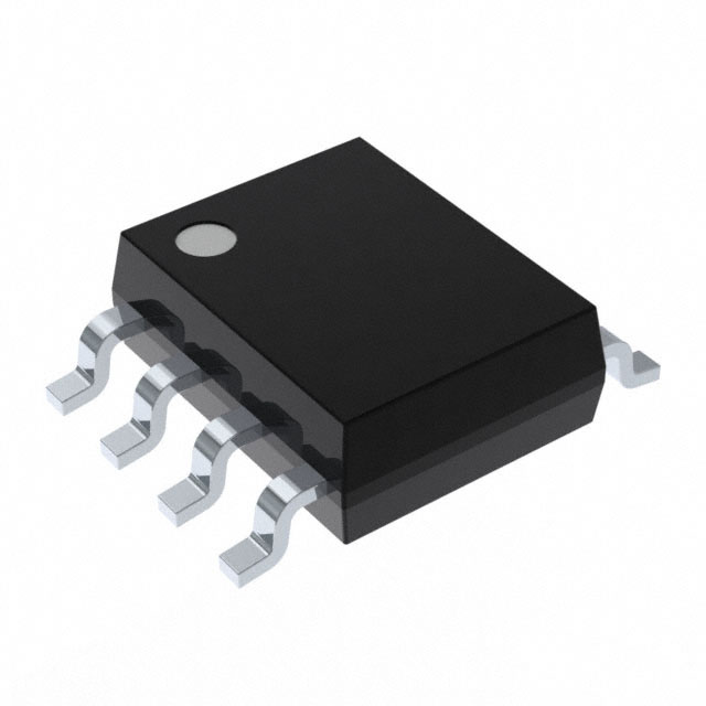
Product Overview: MAX901BCSE-T by Analog Devices Inc./Maxim Integrated
The MAX901BCSE-T represents a versatile quad voltage comparator tailored for high-speed analog signal discrimination. Built upon a differential input architecture, it delivers precise threshold detection with response times conducive to fast analog-to-digital conversion and real-time sampling circuits. The device's design ensures minimal propagation delay, enabling effective operation in timing-critical environments such as instrumentation front-ends, window detectors, and high-frequency pulse extraction systems.
The internal topology integrates TTL-compatible output stages, bridging analog signals to digital logic efficiently. This allows seamless interfacing with downstream microcontrollers and digital processing engines without the need for additional level-shifting components. Its low power profile is advantageous in multi-channel systems, distributed sensing modules, and portable equipment, where both energy efficiency and density matter. By tightly matching input thresholds and optimizing bias currents, process variations are controlled, supporting reliable edge detection in environments susceptible to noise and voltage drift.
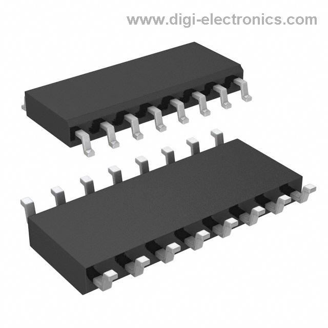
SOIC-16 packaging facilitates straightforward PCB routing, especially for multi-comparator circuit layouts and tightly-packed boards. The pinout symmetry and layout flexibility enable straightforward migration between similar devices within the MAX900–MAX903 series, thus supporting design reuse in established product lines. Nevertheless, as the fabrication process is discontinued, procurement risks emerge for long lifecycles or new deployments; inventory planning becomes essential for sustaining ongoing production, and alternate sourcing strategies should be evaluated during system maintenance or upgrades.
In practical applications, leveraging the device’s fast response time is beneficial in high-speed sampling operations, such as clocked comparators within SAR ADCs, or window comparators for envelope detection in communication circuits. Stability under supply and temperature shifts minimizes recalibration overhead, resulting in predictable in-field performance for industrial and scientific systems. In noise-prone layouts, close attention to PCB component placement and careful selection of supply bypassing can further optimize comparator performance, pushing the boundaries of sensitivity and transient rejection.
The MAX901BCSE-T’s design philosophy prioritizes a balance between speed, power, and interface agility, illustrating the broader trend toward integrated analog-digital bridging elements in modular test, measurement, and control platforms. Its legacy within established series architecture also highlights a lifecycle management challenge: as technologies advance and process discontinuations occur, robust analog interface solutions must blend proven topologies with forward-looking supply chain risk assessment. Ultimately, comparative component selection should not only address immediate technical requirements but anticipate longevity and maintainability in evolving deployment contexts.
Core Features of the MAX901BCSE-T Comparator
The MAX901BCSE-T comparator is engineered for high-speed, low-power signal comparison within demanding electronic systems. Its architecture is tailored to minimize response latency, achieving a typical propagation delay of 8ns at a 5mV overdrive. This rapid response is crucial in scenarios where sub-10ns timing accuracy directly affects system integrity, such as in high-frequency analog-to-digital conversion, fast threshold detection, and stringent timing discrimination in data acquisition hardware.
Power efficiency is achieved without trade-off to performance, with each comparator operating at approximately 18mW when powered by +5V. This low power footprint supports dense multi-channel integration, extends battery life in portable instrumentation, and reduces thermal management overhead in compact embedded designs. The utility of the MAX901BCSE-T becomes more pronounced as system scaling intensifies, where aggregate current draw becomes a critical design constraint.
Flexible input stage design enables the comparator to sense voltages down to the negative supply rail. This feature aids in direct ground-referenced measurements, particularly beneficial in single-supply configurations prevalent in mixed-signal board layouts. Designers can utilize the negative rail sense to streamline analog front-ends, eliminating the need for auxiliary level-shifting or biasing circuits in ground-sensing applications.
Additionally, the device accommodates a wide analog supply voltage range—from +5V to +10V single-supply, or ±5V split rails—while the digital output circuitry is maintained at a consistent +5V. This dual-domain supply arrangement decouples analog responsiveness from digital interfacing, enhancing noise immunity and simplifying mixed-voltage system integration. TTL-compatible output levels directly interface with standard logic families, eliminating further interfacing stages and accelerating development cycles.
From a practical perspective, successful deployment of the MAX901BCSE-T centers on careful PCB layout to mitigate parasitic capacitance at the comparator inputs, which can otherwise degrade high-speed performance. In applications demanding precision low-level comparison, star-grounding techniques and shielded analog traces help preserve signal fidelity. Experience underlines the importance of maintaining clean supply decoupling, particularly when leveraging the extended input range, as transient injection from noisy ground planes may provoke erroneous switching.
While the MAX901BCSE-T is not equipped with a dedicated latch input, some designs may benefit from part selection within the MAX900–MAX903 series to access latched output functionality for sampled-data or clocked applications. This highlights the necessity of matching device features precisely to system timing requirements.
Crucially, the architectural combination of speed, low power, and robust ground-sensing in the MAX901BCSE-T positions it as a compelling solution in measurement instrumentation, communications front-ends, and power management circuits where swift, accurate voltage comparison under resource or board-space constraints is non-negotiable. Balancing these parameters, the device exemplifies efficient analog design, especially where high throughput and low overhead must coexist without compromise.
Electrical Characteristics and Ratings of MAX901BCSE-T
Robust system integration with the MAX901BCSE-T demands precise adherence to its electrical specifications, as these boundaries directly govern stability, reliability, and longevity. The analog supply voltage, capped at +12V between VCC and VEE, establishes the permissible headroom for analog signal operations; exceeding this threshold instigates dielectric breakdown and risks irreversible functional loss. The digital domain is distinctly isolated, supporting up to +7V between VDD and GND, which ensures logic-level integrity and mitigates potential cross-domain noise coupling.
Input voltage tolerance extends from (VEE - 0.2V) to (VCC + 0.2V) for both differential and common-mode signals. This window is engineered to accommodate transients while rejecting undesired bias excursions. Exceeding these bounds provokes input stage latch-up or substrate leakage, translating into unpredictable errata and system-level failures. In precision analog interfacing, enforcing strict compliance within this band prevents offset drift and signal distortion, benefiting applications such as zero-crossing detectors or high-fidelity waveform comparators.
Output protection mechanisms reflect robust design philosophy. Indefinite short-circuit tolerance to ground enables fail-safe operation during prototyping or adverse field events, while the limited tolerance to VDD—strictly one minute—tasks design decisions with careful load planning, particularly in digital driver or active pull-up scenarios. For current steering architectures, careful output trace layout and controlled impedance settlements shield against inadvertent overcurrent exposure.
Thermal management emerges as a critical layer in the engineering approach. The internal power dissipation limit of 500mW, along with the recommendation for derating above +100°C, constrains permissible load and voltage swing profiles, particularly in densely packed assemblies. Failure to manage thermal stress leads to parametric deviations, manifesting in changed offset, propagation delay, or catastrophic device failure. Experience shows that leveraging multilayer PCB layouts with strategic copper pours and thermal vias tangibly reduces die temperature, extending reliable device operation.
Deploying the MAX901BCSE-T across its operational temperature ranges—0°C to +70°C for commercial grade, and -40°C to +85°C for extended grade—positions it for versatility in environmental extremes. Applications in industrial automation or instrumentation benefit from this flexibility, as stable switching and response are maintained under variable ambient conditions. Careful selection of matching temperature grade to system requirements is fundamental to sustaining both accuracy and device lifespan.
In tightly engineered assemblies, treating these ratings as dynamic, context-sensitive variables—rather than static limits—is integral. The interplay between supply and input margins, output protection, and thermal constraints drives a holistic reliability plan. Designs that systematically leverage derating principles and optimize for environmental stress yield measurably superior performance, establishing a direct linkage between rating conformance and field-proven robustness. This layered perspective enables rapid iteration and mitigates the risk of latent electrical fatigue or premature obsolescence.
Functional Architecture and Pin Configuration of MAX901BCSE-T
The MAX901BCSE-T quad comparator integrates four independent, high-speed analog comparison channels within a single 16-pin SOIC package. This architecture enables simultaneous, multi-node signal sensing, which is highly advantageous in systems requiring concurrent threshold detection or distributed analog decision-making, such as industrial controls, sensor arrays, and data acquisition fronts. Each comparator operates with separate differential analog input pairs, enhancing flexibility in processing diverse signal references or operating in environments with varying input common-mode voltages.
The device’s differential analog input structure supports wide common-mode input range management and offsets, permitting robust performance in noisy or low-signal scenarios frequently encountered in measurement and instrumentation systems. Each comparator’s input stage is designed for high input impedance and minimal bias current, supporting direct interfacing with both low and moderate source impedances. This characteristic minimizes distortion and preserves signal integrity, particularly valuable in front-end analog circuits.
Digital output stages adhere to TTL logic thresholds, simplifying direct connection to standard digital logic families. This compatibility streamlines the interface with both microcontrollers and programmable logic devices, eliminating the need for additional level-shifting components. In practical deployment, it is common to utilize the comparators in window detection schemes, hysteresis control applications, and pulse shaping, leveraging the fast response and low propagation delay of the MAX901BCSE-T channels for timing-sensitive analog-to-digital transitions. Experienced designers often parallel unused comparator channels for redundancy or tie their inputs to ground using termination resistors to suppress floating node effects, mitigating potential system noise.
Pin configuration of the MAX901BCSE-T is optimized for efficient board layout. Power and ground pins are sensibly grouped—analog supply and digital supply separated—to support split-rail designs or noise isolation strategies in mixed-signal environments. This arrangement encourages solid decoupling practices by allowing bypass capacitors to be placed close to the supplies, reducing high-frequency power transients. Input and output pins for each comparator are arranged for clear signal routing, simplifying both single-layer and multi-layer PCB layouts and providing straightforward trace planning for analog and digital domains. Special attention to the physical placement of input traces reduces crosstalk and keeps input leakage currents low, critical in precision threshold architectures.
A distinguishing aspect of the device is its standardized footprint and logical pin progression, ensuring drop-in compatibility with legacy quad comparators or facilitating rapid prototyping when design iterations are frequent. The absence of unconventional features—such as shared reference voltages or multiplexed outputs—supports predictable implementation and reliable long-term operation in both cost-sensitive and performance-driven products. The functional architecture underscores a commitment to simplicity, signal integrity, and scalable integration, making the MAX901BCSE-T a practical choice for robust, distributed analog decision circuits.
Performance Considerations and Application Scenarios for MAX901BCSE-T
Performance optimization of the MAX901BCSE-T centers around its high-speed response and minimized quiescent power dissipation, attributes that derive from its advanced comparator architecture and precision biasing circuitry. The device delivers nanosecond-range propagation delays, consistently maintained across operating temperature and voltage variations due to internal compensation techniques. This level of speed directly supports tight timing requirements in analog-to-digital conversion stages, where reliable signal threshold detection is necessary for accurate digital output generation. Integration of the MAX901BCSE-T into A/D converter front ends not only reduces conversion latency but also ensures that high-frequency input signals are sampled without degradation from comparator-induced jitter.
In line receiver applications, the rapid propagation response enables prompt translation of analog voltage transitions into logic-level signals, thus preserving signal integrity across varying cable lengths and EMI-prone environments. The robust common-mode input voltage range, extending to the negative rail, allows seamless interfacing with ground-referenced sources in single-supply systems. Utilizing this rail-to-rail sensing is critical in compact sensor modules and low-voltage control logic where maximizing dynamic range and minimizing layout complexity are priorities.
Voltage-to-frequency conversion circuits benefit from the consistent output toggle behavior provided by tight input offset specifications and symmetrical delay paths within the comparator pair. This stability underpins linearity in frequency output, essential for precision measurement and control in communication systems and signal processing hardware. Data discrimination applications further exploit the accurate toggle threshold and rapid transition capabilities for sorting, gating, or qualifying input data streams in real-time processing environments.
Propagation delay uniformity between dual comparators facilitates parallel operation in multi-channel measurement arrays or synchronised timing circuits. Absence of channel-to-channel skew ensures deterministic logic outcomes in time-critical signal analysis, particularly in modular instrumentation where co-located channels must respond identically to simultaneous input events. Careful PCB layout, with symmetric signal routing and controlled ground returns, amplifies these electrical benefits and eliminates artifacts from stray capacitance or inductive coupling.
Practical deployment recommends coupling the MAX901BCSE-T with low-noise reference voltages and tightly regulated supplies to realize its full resolution and repeatability potential. Embedded systems and test instrumentation have demonstrated measurable reductions in timing errors and power budget overruns when replacing slower, higher-consumption comparators with the MAX901BCSE-T, leading to enhanced throughput and reliability in dense analog front ends. Selective use of ground-referenced sensing in logic-level resistor ladder networks and mixed-signal boards addresses long-standing interoperability challenges, expediting signal qualification without added buffering stages.
Strategically, the architectural emphasis on symmetrical delay, low input offset, and rail-to-rail operation offers unique deployment flexibility, supporting both traditional analog roles and emerging digitally assisted measurement tasks. These capabilities inherently drive design choices towards more compact, power-efficient, and high-fidelity system implementations, streamlining signal chain complexity while elevating timing and threshold performance metrics throughout a diverse range of real-world scenarios.
Circuit Design Guidelines for MAX901BCSE-T
High-speed comparators such as the MAX901BCSE-T present distinct challenges in circuit design, particularly regarding PCB layout and signal integrity. Effective performance hinges on controlling noise and minimizing parasitic effects originating from layout decisions and component selection.
At the foundation, robust ground plane strategies are critical. Employing a contiguous, low-inductance ground plane underneath the comparator mitigates common-mode noise susceptibility and enables consistent return paths for high-frequency signals. In tightly packed circuits, ground flooding beneath the device with well-placed vias minimizes impedance disturbances and enhances electromagnetic compatibility. High-frequency noise coupling is common through ground impedance loops; careful plane segmentation and via stitching address these effects, ensuring stable baseline voltages.
Power distribution demands precise decoupling approaches. Each supply pin, analog and digital, requires its own low-ESR ceramic bypass capacitor—commonly 100nF X7R types—placed within a few millimeters of the respective pin. This localized energy storage counters fast transient currents generated during switching events, enhancing settling performance. Maintaining dedicated supply decoupling for analog and digital rails eliminates cross-domain noise propagation, a frequent root of output glitches and increased comparator response time.
Signal integrity benefits significantly from minimizing trace lengths and parasitic stray capacitance at the input and output nodes. Traces should be as short and direct as practical, using controlled-impedance routing where transition rates are sub-nanosecond. Excessive trace length or stubs can degrade signal fidelity through distributed capacitance and inductance, contributing to false triggering, propagation delay, and error susceptibility. Integrating the comparator device directly onto the PCB, rather than socketing, further reduces effective lead inductance, a nontrivial source of high-frequency error in fast comparators. Soldered connections yield lower and more predictable impedance, which aids in repeatable, high-speed system behavior.
Input signal conditioning directly impacts the comparator’s output stability. Adequate input slew rate must be maintained—not only to meet datasheet limits, but also to account for degraded performance stemming from high source impedance or suboptimal trace geometry. Upstream drivers must deliver transitions sufficiently faster than the minimum required; verification at the PCB level is indispensable, particularly at or near switching thresholds, where even modest underperformance can manifest as chatter or oscillation.
Hysteresis, commonly implemented via positive feedback in the input network, serves as a vital countermeasure where noisy or slow input transitions are present. Appropriately sized hysteresis loops immunize the output against minor perturbations and supply variance, sharpening threshold behavior. In cases of persistent instability or burst oscillations, small-value resistive networks between output and non-inverting input can often provide the necessary offset, tailored for the application’s noise floor and switching speed.
These guidelines are not merely theoretical; adherence materially impacts the repeatability and robustness of high-speed comparator circuits. In precision measurement applications, minute layout refinements—such as relocating a via path or substituting for a lower-inductance capacitor package—often translate into measurable improvements in propagation delay and offset error. The benefits compound in high-density analog front ends, where interactions between comparator devices can generate subtle crosstalk or edge jitter if supply and ground strategies are marginal.
Practical deployments frequently reveal that design compromises, such as shared decoupling or relaxed trace constraints, degrade comparator fidelity in unanticipated ways. Therefore, applying rigorous simulation and post-layout validation, including oscilloscope probing of supply pins and outputs under real operating conditions, adds assurance that theoretical performance targets are actually realized in hardware.
Optimized comparator design is ultimately achieved by layering meticulous layout discipline, proactive noise countermeasures, and context-specific signal conditioning. The interplay of these practices yields high signal accuracy and reliable speed, enabling systems to leverage the MAX901BCSE-T's full high-speed comparator capability with minimal susceptibility to board-level artifacts.
Power Supply Options for MAX901BCSE-T
Power supply configuration critically influences the precision and noise performance of the MAX901BCSE-T comparator. The device’s analog supply is versatile, supporting single-supply operation from +5V up to +10V, as well as dual-supply configurations (±5V), which can be advantageous when negative signal handling or improved common-mode range is required. Selection between these modes must align with the application’s dynamic range requirements and system-level grounding topology. Notably, the digital supply is limited to +5V, independent of the analog domain’s voltage, simplifying integration into standard logic environments while providing robust logic level compatibility.
The decoupling strategy for both analog and digital rails deserves careful consideration. Direct placement of low-ESR ceramic capacitors (e.g., 0.1µF) close to device supply pins mitigates high-frequency transients, reducing susceptibility to supply-borne jitter and spurious switching. In low-noise systems, a larger bulk capacitor (e.g., 10µF tantalum) stabilizes the analog rail against load variations. Isolation of analog and digital supplies, when feasible, prevents high-frequency digital activity from corrupting sensitive analog thresholds.
In the context of mixed-signal PCB layouts, distinct analog and digital ground planes (AGND and DGND) are essential. Linking these planes at a single point near the device enforces a controlled current return path, minimizing ground loops and enhancing noise immunity. Empirical observation confirms reduced cross-domain interference when the comparator straddles the boundary between AGND and DGND, with analog inputs referenced exclusively to AGND. Special care is required to route digital outputs directly toward DGND domains to limit capacitive coupling into the analog region.
From a system integration perspective, maintaining a low-impedance path for both grounds and supplies ensures stable comparator thresholds under fast switching conditions. Board-level test results show that neglecting either power supply isolation or local decoupling often produces erratic toggling or drift in switching levels, especially under burst signal environments common to data acquisition front-ends. Therefore, deliberate supply segmentation and careful grounding provide a measurable improvement in signal fidelity and device reliability.
This power delivery strategy, while generalizable, takes on increased importance as switching speeds and input sensitivity rise. Practical layouts balance close physical proximity of bypass capacitors, unbroken ground planes, and minimal supply trace inductance. These techniques collectively form a foundation for robust comparator performance across diverse instrumentation, signal conditioning, and mixed-domain interface scenarios.
Potential Equivalent/Replacement Models for MAX901BCSE-T
With the discontinuation of the original wafer process for the MAX901BCSE-T comparator, a shift in sourcing strategy becomes essential for maintaining design timelines and ensuring long-term availability. The primary engineering concern centers on minimizing redesign effort while upholding system specifications, such as propagation delay, input thresholds, and output drive capability. Identifying drop-in replacements requires a critical assessment not only of electrical equivalence but also of operational nuances under varied application stresses.
Pin-compatible successors from Maxim Integrated, namely the MAX9201, MAX9202, and MAX9203, directly address this scenario. Their logic-level compatibility and near-identical performance benchmarks facilitate straightforward substitution at the PCB level. Notably, these devices exhibit superior power efficiency—a metric increasingly prioritized in densely integrated systems and battery-powered applications. Reduced quiescent currents directly translate to fewer thermal management constraints and extended operational longevity in portable equipment.
Analyzing the core architectural enhancements reveals differentiated input stage design and internal bias optimization in the replacement series, yielding improved input offset and lower power profiles without sacrificing switching speed. This design choice also enhances tolerance to voltage transients and supply fluctuations, leading to improved stability in noisy environments such as automotive and industrial control systems.
In deployment, adopting these replacements has demonstrated seamless transition in high-frequency signal conditioning circuits, where maintaining propagation delay and low input bias currents are mission-critical. Subtle variances in input capacitance or common-mode voltage range should be scrutinized, especially for precision analog front-end designs or mixed-signal applications interfacing with sensitive ADCs. Field experience shows that comprehensive validation—especially under full-temperature sweeps and across supply bounds—confirms reliable performance parity or, in some edge cases, marked enhancement over legacy parts.
Proactively incorporating second-sourced or cross-verified comparator models is a best practice, guarding against further obsolescence and unexpected lifecycle disruptions. Extending this approach, leveraging parametric equivalence databases and maintaining robust communications with component manufacturers optimizes risk mitigation for future platform updates. Carefully curated substitutions such as the MAX920x series not only streamline migration from end-of-life components but also align with industry trajectories toward lower power, higher reliability mixed-signal design.
Conclusion
The MAX901BCSE-T, a quad comparator designed for high-speed signal discrimination, integrates critical performance parameters—fast propagation delay, low quiescent current, and rail-to-rail compatibility—delivering effective solutions for analog front-end designs in instrumentation and communication systems. Its architecture supports simultaneous multi-channel processing, facilitating coherent threshold detection across parallel analog inputs. The internal comparator design leverages matched bipolar input pairs, minimizing input offset and ensuring precise output transitions under rapid signal variations, which is crucial when system time constraints and noise margins are stringent.
From a supply perspective, the device accommodates a wide voltage range typical for industrial and data acquisition contexts. Stability on the supply rails, careful decoupling, and minimizing impedance along power traces reduce susceptibility to transient voltage drops, which can otherwise produce unintended toggling or degrade response fidelity. In PCB layout, strict attention to input trace symmetry and cross-talk isolation remains essential, especially where dense analog routing and high-speed logic coexist. Input pins should be shielded from aggressive digital signals, and optimal ground referencing via local star points can attenuate common-mode disturbances, leveraging the comparator’s common-mode rejection capabilities.
Given the “not recommended for new designs” (NRND) status, lifetime component availability emerges as a decisive integration factor. Risk–benefit analysis dictates favoring the MAX901BCSE-T predominantly for maintenance or extension of legacy hardware, where pin-, logic-, and parameter-compatibility outweighs long-term sourcing threats. For such scenarios, continuity of analog behavior and drop-in equivalence across board revisions outvalue the uncertain future of supply chains. In contrast, next-generation product development should prioritize migration paths toward the MAX920x family or proven peers, where long-term vendor support and enhanced process nodes ensure greater design resiliency. Notably, subtle differences in propagation delay, input bias currents, or power dissipation profiles between candidate comparators may require empirical validation in-system; bench measurements during qualification often reveal dynamic nuances unobservable from datasheets alone.
Critical engineering experience demonstrates that small deviations in input signal integrity—unintended voltage offsets or transients—can disproportionately affect high-speed comparator behavior, especially in mixed-signal environments. Meticulous signal conditioning and robust filter design on sensitive analog nodes markedly improve comparator switching fidelity. In factory automation, for example, even microvolt-level ground bounce or inadequate filtering upstream can precipitate false triggering, impacting control algorithms and downstream data interpretation. Tuning hysteresis externally via resistive feedback, or leveraging integrated hysteresis features where available, suppresses response to minor fluctuations and ensures reliable discrimination in noisy conditions.
Ultimately, while the MAX901BCSE-T offers a compelling balance of speed, power economy, and channel density for sustaining legacy designs, forward-looking projects demand a comprehensive evaluation of long-term availability. Layering supply chain foresight onto circuit design principles yields robust systems adaptable to changing process technologies, underlining the need for vigilant engineering due diligence throughout the component selection phase.