 >
>


Product overview of the AD8400AR1 Analog Devices digital potentiometer
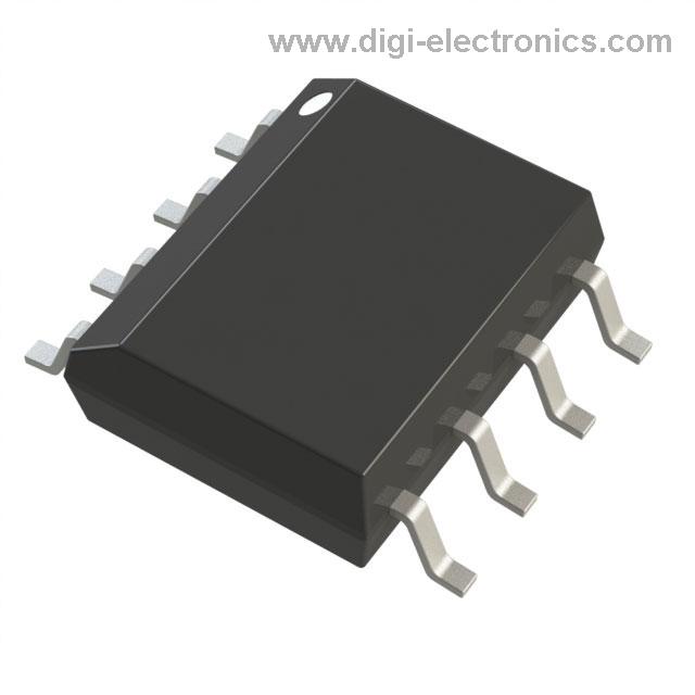
The AD8400AR1 digital potentiometer from Analog Devices functions as a 256-position, SPI-controlled variable resistor, emphasizing precise electronic signal tuning and circuit parameter adjustment. Its core architecture replaces mechanical potentiometers with a solid-state solution, eliminating wear issues and drift while introducing robust programmability. Integrated into an 8-lead SOIC package, the device offers a single 1 kΩ channel, ideal for compact applications where board space and component count are critical.
At the substrate level, the AD8400AR1 utilizes a resistor array and digital decoding logic that maps serial data inputs to discrete resistance steps. The SPI interface streamlines seamless communication with microcontrollers, FPGAs, or embedded processors, facilitating real-time resistance modifications without physical intervention. This eliminates the variability inherent to manual trimming and supports automated calibration during both production and system operation. Embedded non-volatility ensures set values are retained through power cycles when paired with appropriate external memory strategies.
From an electrical perspective, the 2.7 V to 5.5 V operating range strengthens compatibility across low-voltage and standard digital platforms. The low quiescent current (<5 μA in shutdown) supports battery-powered designs and energy-conscious modules, making the device suitable for remote sensor nodes, portable instrumentation, and distributed control networks. The wide-range resistance portfolio within the AD840x family, spanning from 1 kΩ to 100 kΩ, provides engineers with fine granularity for tailoring RC filter, gain, and offset topologies in analog front ends.
Noise immunity stands out due to the absence of mechanical contacts, lowering susceptibility to environmental vibrations, dust ingress, or oxidation. In electromagnetic-intensive settings, such as industrial automation or vehicular subsystems, the stability of the resistor network fosters consistent analog performance even under fluctuating load and signal conditions. Application domains include programmable gain amplifiers, voltage dividers for reference circuits, sensor signal conditioning, and digital control for LED drivers or audio attenuation. Field deployment highlights rapid prototyping cycles and straightforward integration into existing bus architectures, reducing both system complexity and maintenance intervals.
Mechanical potentiometer replacement extends beyond reliability—programmable digital potentiometers like the AD8400AR1 accelerate recalibration routines and support dynamic system adaptation, such as temperature-dependent compensation or remote configuration in distributed networks. The device's deterministic resistance steps enable fine-tuned control, lending themselves to closed-loop feedback mechanisms in precision instrumentation and control algorithms.
The intersection of flexibility, endurance, and clean signal integrity in the AD8400AR1 can be leveraged further through custom firmware support, allowing dynamic re-assignment of resistance values in response to environmental inputs or operational telemetry. This capability transforms static designs into adaptive systems equipped to handle evolving requirements or in-field updates, a key advantage in contemporary engineering contexts emphasizing modularity and scalability.
Functional and electrical characteristics of the AD8400AR1
The AD8400AR1 integrates a resistance ladder trimmed for linearity and fine step resolution, forming the basis of its digitally controlled potentiometer architecture. By leveraging a 256-position tap, the device offers precise, monotonic adjustment from 0 Ω to nominal end-to-end resistance, facilitating analog signal conditioning with microcontroller-level digital interface. The wiper mechanism is constructed to deliver consistent transition between steps, with integral nonlinearity (INL) and differential nonlinearity (DNL) consistently maintained within 1 LSB. This precise quantization ensures minimal distortion, a critical factor for applications involving programmable gains or threshold adjustments.
Focusing on electrical performance, the component specifies a 1 kΩ total resistance per channel, tightly matched within ±1%—crucial for multi-channel parallel deployment where systematic error can cascade across a signal chain. The temperature coefficient of 500 ppm/°C ensures resistance value stability across a wide thermal range (-40°C to +125°C). This characteristic supports deployment in both automotive and industrial control environments, where thermal shifts routinely stress passive networks. In low-scale settings, the typical wiper resistance is pegged near 50 Ω, a factor that requires attention during low-voltage or precision analog design to avoid inadvertent loading and IR drop.
The device’s protection circuits are robust, with electrostatic discharge (ESD) resilience aligned with stringent JEDEC criteria. This directly enhances operational reliability when board- or system-level disturbances cannot be fully mitigated. Limiting wiper-to-terminal current to 5 mA is recommended to prevent stress on internal CMOS transmission gates, preserving both linearity and operating life. Observed in real-world bench validation, current excursions beyond this threshold can induce both resistive drift and momentary nonlinear glitches, underlining the importance of careful current budgeting in mixed-signal layouts.
Power management is realized through sub-10 μA supply current in shutdown scenarios, contributing minimal parasitic loading in battery-sensitive or low-quiescent current architectures. The logic interface is constructed for standard CMOS compatibility, enabling straightforward integration with low-power embedded controllers. In test implementations, toggling the logic-controlled shutdown has consistently reduced active power without side-effects on resistance programming integrity—valuable for dynamic power scaling or remote sensor modules.
Much of the device’s strength materializes when deployed in calibration, trimming, or feedback paths where in-circuit adjustability is paramount. For instance, supporting automated offset calibration in closed-loop amplifiers is streamlined by the digital addressability of the wiper, and the monotonic response allows fractional adjustments with repeatable accuracy. Furthermore, reliance on CMOS technology underpins the component’s compact footprint and thermally stable logic thresholds, which enable high packing density on dense PCBs without susceptibility to latch-up or leakage under adverse environmental conditions. Success in these domains relies on a clear appreciation of both the functional resistance characteristics and nuances in interfacing, particularly with regard to the constraints imposed by wiper resistance and permissible terminal currents. This nuanced understanding enables optimization of both analog performance and component life expectancy.
Fundamentally, the AD8400AR1 achieves a balance between precision, programmability, and ruggedized operation. An application-aware approach—respecting its electrical boundaries and leveraging its fine gradation—ensures consistently reliable performance across diverse engineering contexts.
Programming and digital interface in the AD8400AR1
The AD8400AR1 leverages a streamlined 3-wire SPI-compatible interface, utilizing Chip Select (CS), Serial Clock (CLK), and Serial Data Input (SDI) lines for effective digital control. At the protocol level, programming operates through a 10-bit data frame: the initial two bits serve as the address phase—preset for single-channel configurations—while the subsequent eight bits directly encode the wiper’s resistance value. This approach simplifies the integration process in tightly constrained processor environments, as it reduces code and timing overhead often encountered with more complex communication schemes.
Underlying interface mechanisms are engineered to support robust and responsive system interaction. The device tolerates serial clock speeds up to 10 MHz, substantially decreasing resistance update latency, critical for applications demanding rapid analog parameter modulation such as real-time signal processing or programmable gain amplifiers. The monotonic nature of increment/decrement actions in wiper positioning bolsters system reliability by eliminating non-deterministic transitions, a factor essential in control systems where predictable behavior is mandatory.
A practical advantage lies in the device’s auxiliary reset (RS) and shutdown (SHDN) pins. The reset function restores the wiper to midscale without cycling power, enabling consistent startup states and efficient test sequences during field deployment or automated production testing. The shutdown capability disconnects the output to yield a power-saving, high-impedance state, while internal registers retain their last command, allowing seamless resumption of previous settings post-standby. This architecture is highly suited to battery-powered and remote-controlled systems, where minimizing energy consumption and ensuring prompt return to operation are central requirements.
Advanced scenarios reveal further utility. The AD8400AR1 design supports daisy-chaining, facilitating scalable multi-device configurations with minimal additional wiring. While more prevalent in the multi-channel AD8402/AD8403 variants, the foundational support remains valuable when constructing modular analog front-ends that demand precise, software-driven trimming across distributed nodes. This feature is especially useful in automated adjustment and calibration routines within distributed sensor arrays, where synchronized updates of several potentiometer elements are necessary.
Programming the AD8400AR1 yields operational flexibility absent from traditional manual potentiometers. Dynamic, real-time resistance control becomes practical both locally and over networked links, streamlining iterative optimization in embedded platforms, industrial automation, and adaptive analog filtering. The interface’s simplicity effectively lowers firmware complexity and shortens development cycles, while the device’s robust state retention methods enhance system resilience during power interruptions or sleep mode transitions.
This convergence of fast digital interface, deterministic wiper control, and power-aware features underscores a paradigm shift in mixed-signal design. Precision analog adjustment merges seamlessly with digital programmability, reducing calibration time and error while enabling new adaptive and self-tuning application domains.
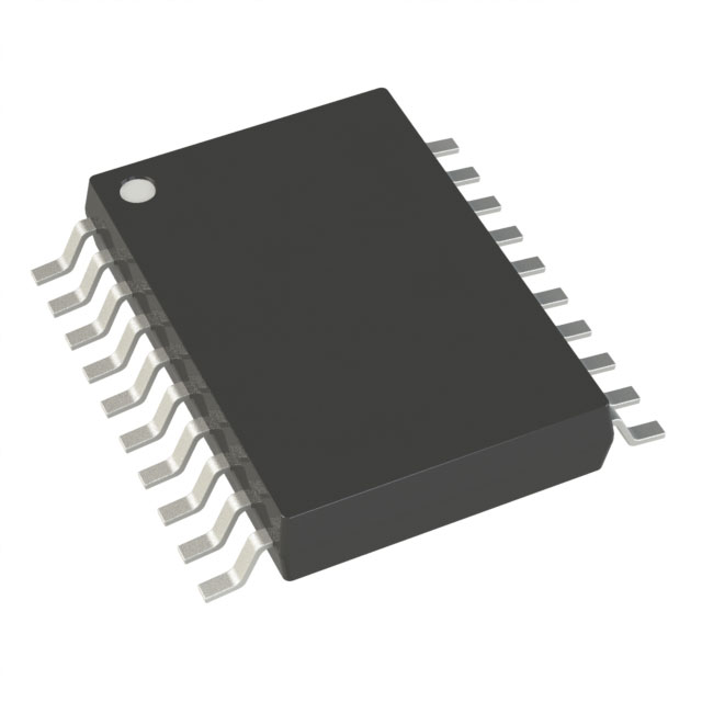
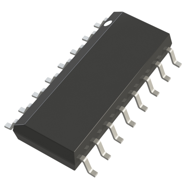
Package options and mechanical dimensions of the AD8400AR1
The AD8400AR1 employs an 8-lead SOIC package that strictly adheres to the JEDEC MS-001 standard, a format chosen for its proven reliability in surface-mount manufacturing environments. This mechanical specification, typically measuring 4.90 mm × 3.91 mm (0.193 in × 0.154 in), provides cross-regional compatibility and straightforward integration into automated pick-and-place operations, minimizing the risk of assembly errors and supporting high-throughput board designs. The precise package dimensions facilitate dense PCB layouts required in modern mixed-signal systems, where space constraints and signal integrity are pivotal in multi-layer architectures.
Selecting the SOIC-8 package directly supports legacy replacement scenarios, especially where migration from traditional mechanical potentiometers or alternative digital potentiometer brands is necessary. Pin-to-pin compatibility and consistent soldering profiles reduce engineering validation overhead, streamlining qualification cycles in both new and retrofit product releases. It is common in practice to exploit the standardized lead pitch and coplanarity tolerances of SOIC-8 packages to reduce failures in reflow soldering, thus improving long-term field reliability.
Expanding within the AD840x product line, multi-channel variants such as the AD8402 and AD8403 offer additional package options, including SOIC-14, PDIP-14, TSSOP-14, PDIP-24, SOIC-24, and TSSOP-24. These choices enable flexibility in system partitioning, allowing designers to optimize for either board real estate or conventional through-hole prototyping, depending on project phase and volume targets. For instance, TSSOP packages present a lower profile, essential for vertically constrained enclosures, while PDIP facilitates socketed prototype arrangements and expedites debugging. SOIC-24 and TSSOP-24 open avenues for integrating higher channel counts into compact footprints, supporting increased functionality without sacrificing mechanical stability or assembly yield.
When optimizing for manufacturability and field scalability, the well-documented thermal and electrical characteristics of these packaging options prove advantageous. Consistent lead-frame geometries enable straightforward thermal simulation and accurate derating in high-density power distribution environments. Moreover, leveraging the familiarity of JEDEC-compliant outlines across multiple variants reduces supply chain risk and accelerates time-to-market by enabling multi-sourcing strategies—an often overlooked yet critical aspect in robust system development.
A key insight is the strategic alignment between package selection and long-term maintainability. By standardizing on a JEDEC mechanical outline and dimension set, design teams avoid the pitfall of packaging obsolescence, which can disrupt lifecycle management in larger deployments. It is advisable to evaluate channel scalability and mechanical constraints early in the system architecture phase, as this ensures clear migration paths and mitigates potential redesign cycles during scaling or cost-reduction efforts. This holistic approach to package engineering not only boosts efficiency but also futureproofs product lines in dynamic market environments.
Operation theory and performance considerations with the AD8400AR1
The AD8400AR1 operates as a digitally controlled variable resistor, featuring a precisely engineered resistor chain gated by solid-state switches. The internal architecture enables interpolation across 256 discrete tap points, spanning from 0 Ω to 1 kΩ, with an incremental step size defined by the digital input code. Wiper resistance is inherent to the switching mechanism, typically in the tens of ohms, and must be considered in low-resistance applications for accurate modeling and system integration.
Core modes of operation derive from different terminal configurations, each with distinct circuit implications. In rheostat mode (2-terminal configuration), the wiper serves as a programmable resistor between one terminal and the common node, facilitating flexible current regulation, tunable RC networks, or oscillator timing adjustments. Direct control via SPI-compatible logic supports rapid resistance updates, allowing dynamic adaptation in feedback loops, automatic level controls, or sensor calibration procedures. The linearity of the resistance adjustment is fundamentally determined by the resistor string uniformity and switch parasitics, underscored by a repeatable step response. Practical experience demonstrates that, in low-impedance environments, additional series resistance due to the wiper can be mitigated by calibrating zero-code offsets in software.
Potentiometer divider mode leverages all three terminals, configuring the AD8400AR1 as an electronically adjustable voltage divider. Applications benefit from the intrinsic ratio accuracy, which relies on the matching properties of the resistor string rather than absolute resistance tolerance. This architecture sharply reduces susceptibility to thermal drift and non-linear error, yielding robust performance in programmable gain amplifiers, adaptive filter designs, and voltage reference adjustment blocks. Real-world deployment reveals enhanced thermal performance under matched resistor conditions; when environmental temperature varies, system designers can rely on the stability of the divider ratio, markedly improving precision in sensitive analog processing chains.
Bandwidth characteristics align closely with the selected resistance value; for instance, the 10 kΩ variant achieves -3 dB bandwidths approaching 600 kHz. Higher resistance settings result in lower bandwidth, a direct consequence of increased RC time constants. This factor becomes crucial in high-frequency analog signal paths, requiring designers to select resistance values judiciously for optimal performance. The architecture supports low total harmonic distortion, maintaining signal integrity in audio circuits and high-fidelity sensor interfaces. Burn-in reliability is underpinned by the solid-state nature of the switching elements; extended operation and cycling do not materially degrade resistor string integrity or digital control performance.
When deploying multiple channels in parallel, crosstalk minimization is evident through both die layout and shielding strategies, critical where isolation and low noise are essential. The inclusion of robust ESD structures across all pins provides resilience against transient disturbances during assembly and operation, while the supply voltage compatibility ensures flawless integration in complex mixed-voltage systems. In practice, these protective features substantially reduce device casualties during prototyping and field deployment, minimizing downtime and calibration effort.
Through a deep understanding of the underlying mechanisms—switching action, resistor matching, and layout optimizations—engineers can harness the AD8400AR1’s capabilities across a wide spectrum of programmable analog tasks. System flexibility, analog precision, and digital control convergence define its application strength, with nuanced considerations for parasitics and operational bandwidth guiding optimal design choices. In precision tasks, leveraging the ratio stability of the divider mode and compensating for wiper offsets in rheostat mode yield solutions with repeatable, robust performance. The device stands out as a reliable component for configurable analog networks, where speed, accuracy, and integration are paramount.
Application scenarios for the AD8400AR1 digital potentiometer
The AD8400AR1 digital potentiometer is optimized for implementing flexible, precision-controlled resistance networks across a range of signal chain and system-level architectures. Its core functionality—digital programmability—fundamentally transforms traditional potentiometric roles, replacing mechanical elements with solid-state reliability and control. This transition eliminates issues like contact wear, drift from vibration, and the need for manual recalibration while ensuring consistent resistance values across repeated cycles and extended lifetimes.
In programmable filtering and timing solutions, the AD8400AR1 serves as an adjustable resistor element within RC and active filter assemblies. By modulating resistance values digitally, circuit designers can reconfigure cutoff frequencies or delay constants dynamically, supporting applications in reconfigurable radio and signal processing platforms. The integration of register-based control delivers deterministic, low-latency adjustment in response to firmware algorithms or system events—a principle leveraged to implement adaptive communication protocols and multiplexed signal paths.
The precision-grade digital manipulation of resistance enables remote and granular audio level control systems, including volume and pan operations. This capability extends from embedded consumer products to professional audio consoles, supporting both incremental adjustment and complex recall functionalities. The potentiometer’s nonvolatile register system sustains last-used settings across power cycles, simplifying user experience and integration with control networks.
In transmission line and bus architectures, AD8400AR1 allows dynamic impedance matching and termination, critical for preserving signal integrity under variable loading or link configurations. This adaptability is instrumental in modern automated test setups, where channel characteristics often shift in real time. Precise programmable resistance facilitates consistent network calibration without hardware changeovers, aligning with industry trends toward modular and software-defined instrumentation.
Power supply calibration tasks benefit from the device’s capacity to fine-tune feedback and reference elements within voltage regulation circuits. Programmatic access to these points supports remote diagnostics, rapid prototyping, and even field upgrades, underscoring the efficacy of digital trimmers in distributed control scenarios.
In more advanced design topologies, AD8400AR1 is frequently embedded within digitally controlled gain stages and analog front end conditioners. The capacity for on-the-fly adjustment supports sensor linearization and auto-zero techniques, aligning with trends in self-calibrating measurement and control systems. Directly coupling these elements with microcontrollers or DSPs enables fine-tuned responses based on environmental sensing or algorithmic feedback, yielding significant reductions in setup and maintenance times.
Deployments in industrial automation, automotive control, and harsh environments leverage the component’s robust operational envelope, including extended temperature tolerances and vibration resistance. This reliability shifts calibration and tuning paradigms toward remote, software-driven routines, substantially reducing intervention frequency and downtime in safety-critical and mission-driven applications.
The greatest value emerges by considering system-level programmability as not merely a replacement for manual controls, but as a foundation for adaptive, self-optimizing electronics. By embedding programmable potentiometric elements directly in control and measurement chains, architectures can evolve toward increased autonomy, supporting feature migration, remote diagnostics, and dynamic reconfiguration in deployed systems. This broadens the options for real-time optimization and asset management, reflecting a subtle yet powerful shift in how resistance networks are specified and employed within high-performance embedded solutions.
Potential equivalent/replacement models for the AD8400AR1
Identifying functionally equivalent or replacement models for the AD8400AR1 requires a multi-faceted evaluation centered on electrical performance, interface integration, and compatibility. The AD8400AR1, a single-channel, SPI-compatible digital potentiometer, is selected in applications prioritizing programmable resistance with fine control and robust digital interfacing. The cornerstone parameters guiding alternative selection involve resistance value, total tap positions, interface logic levels, package outline, temperature tolerance, and, crucially, matching and end-to-end resistance accuracy.
Within the AD8400 family, alternate resistance values—such as 10 kΩ (AD8400AR10), 50 kΩ (AD8400AR50), and 100 kΩ (AD8400AR100)—offer drop-in flexibility where only the nominal resistance differs. This homogeneous architecture guarantees consistent pin mappings, binary command protocol, and thermal performance. Such intra-family substitution streamlines the adjustment process during late-stage prototyping or minor design updates, eliminating qualification overhead associated with new part footprints or firmware modifications.
For multisignal control or increased channel density, parts like the AD8402 (dual channel) and AD8403 (quad channel) offer parallel scalability. These devices unify multiple independent potentiometers within a reduced PCB footprint, optimizing board layout in embedded control or signal conditioning modules. Designs emphasizing analog front-end integration or minimizing interconnect complexity benefit from these variants, provided that supply voltage, package thermals, and bandwidth remain within the host system’s constraints.
When cost, resolution, or size become driving factors, functional equivalents such as the AD5160—also from Analog Devices—provide a compelling Single-channel 256-tap architecture, at times surpassing the 256-position granularity of the AD8400 series. Adjustments in interface timing or startup programming may be necessary, but these models offer consistent SPI command structure and supply voltage ranges. This approach serves applications such as consumer electronics, where budget and component count must be tightly managed without sacrificing programming precision.
Extending to competitor offerings, solutions from Microchip (MCP41xxx/42xxx) and Maxim Integrated (DS1803) introduce alternatives with broad resistance selections and similar SPI interfacing. Successful integration is contingent on analyzing key electrical parameters: wiper resistance, total resistance tolerance, programming voltage thresholds, and timing protocols. Even with nominal pin-for-pin package compatibility, attention to signal sequencing, absolute maximum ratings, and power-on-reset behaviors is essential. Also, unforeseen discrepancies in temperature coefficients or ESD hardness may necessitate bench validation or board-level modifications.
Specialized environments, particularly automotive, enforce qualification metrics such as AEC-Q100. The “W” grade variants within the AD8400/2/3 range specifically satisfy this criterion, sustaining reliability under extended temperature cycles and vibration. Project experience highlights the importance of explicitly confirming grade designations during procurement, especially in supply-limited scenarios where confusion between standard and automotive-qualified stock is common.
In summary, model substitution for the AD8400AR1 is not a mere part-number exercise but a convergence of system-level requirements. Nuanced trade-offs arise around wiper performance, channel density versus layout flexibility, and the implications of qualification standards. Layered analysis—from pinout compatibility and protocol adherence up to environmental and application-class compliance—delivers robust design resilience and promotes long-term system reliability. Strategic use of internal family variants accelerates the process, while measured integration of cross-manufacturer parts broadens sourcing, provided rigorous interface and performance verification is maintained throughout the design cycle.
Conclusion
The AD8400AR1 embodies the evolution of digital potentiometer technology, delivering precision, repeatability, and seamless electronic control for analog signal conditioning. Its architecture features a digitally selectable resistor ladder, interfaced via an industry-standard SPI-compatible serial bus. This approach enables real-time adjustment of resistance values, eliminating mechanical variability, contact wear, and the challenges of physical calibration. The device's nonvolatile wiper storage ensures reliable state retention through power cycles, enhancing stability in mission-critical circuits.
Electrical characteristics of the AD8400AR1 illustrate its suitability for high-density, low-power designs. With low supply current draw and wide voltage tolerance, the device integrates efficiently into both legacy and modern mixed-signal systems. The resistance tolerance and temperature coefficients are engineered to meet stringent precision requirements, minimizing drift and enabling stable operation across variable environmental conditions. Attention to ESD robustness and latch-up immunity further improves reliability during manufacturing and field deployment, especially in automotive and heavy-duty industrial scenarios.
Design-in of the AD8400AR1 calls for thoughtful interfacing to optimize signal integrity and programmability. Pin mapping supports direct connection to microcontrollers, FPGAs, or dedicated analog front-ends, while the compact SOT-23 packaging maximizes board area savings. PCB layouts should be routed carefully to minimize parasitic effects and digital crosstalk, with consideration for ground planes and decoupling. In prototyping, precise voltage measurements across the end terminals confirm linearity and performance under dynamic digital inputs—a key metric for feedback and gain-control circuits.
Real-world deployments reveal the device’s strengths in field calibration, programmable voltage dividers, audio attenuation, and sensor trim functions. In instrumentation, remote resistance adjustment is executed without physical intervention, reducing downtime and enabling adaptive compensation routines. Consumer systems, such as smart home controllers, benefit from silent, wear-free operation, with configuration stored persistently to streamline user experience and reduce post-install maintenance. Automakers leverage AD8400AR1 in distributed electronic control units, where compactness and reliability simplify harnessing and ensure fault tolerance in distributed environments.
The convergence of reliability, electrical performance, and digital control positions the AD8400AR1 as a strategic choice for scalable analog signal solutions. Integration facilitates predictive maintenance, fine-grained analog modulation, and enhanced configurability—attributes increasingly valued in industrial automation and edge-node architectures. Selecting AD8400AR1 enables efficient development cycles and robust real-world performance, driving measurable advances in system flexibility and overall engineering value.