 >
>


Product overview: AD7916BRMZ-RL7 from Analog Devices Inc.
The AD7916BRMZ-RL7, engineered by Analog Devices Inc., represents a high-performance solution in the domain of analog-to-digital conversion. At its core, the device employs a successive approximation register (SAR) architecture, enabling 16-bit resolution with low latency. SAR topology optimizes both conversion speed and accuracy by iteratively refining each bit decision, avoiding cycles of oversampling and decimation. This method guarantees deterministic timing—critical for closed-loop control, industrial automation, and precision instrumentation where response consistency is non-negotiable.
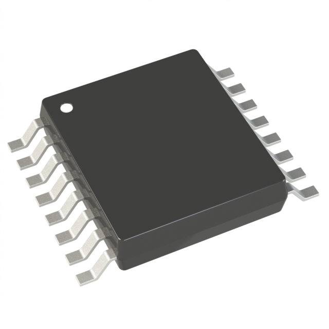
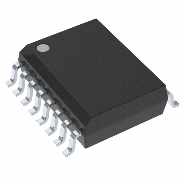
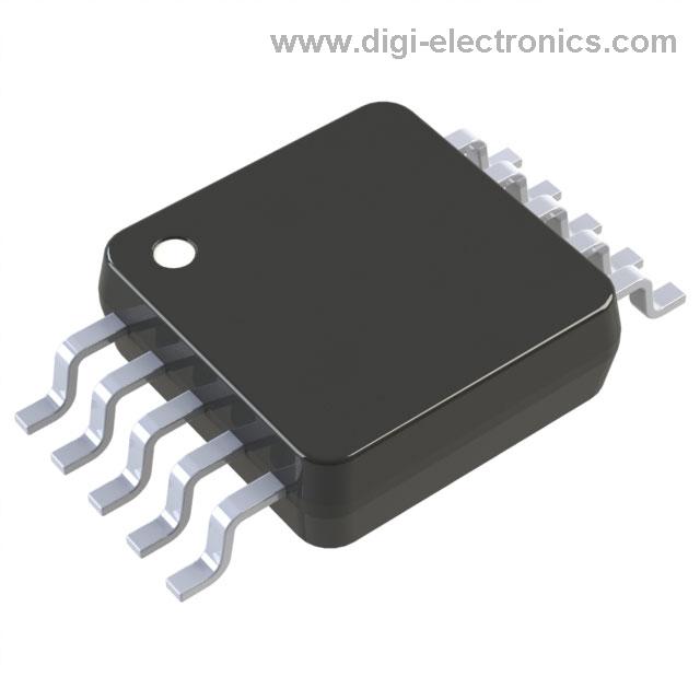
Behind its compact 10-pin MSOP package, the AD7916BRMZ-RL7 integrates features essential to precision signal acquisition. Its single-input configuration reduces internal switching artifacts and crosstalk, minimizing system-level uncertainties that commonly challenge multi-channel architectures. High linearity and low noise floor are achieved through careful analog front-end design, ensuring that input signals translate into stable, monotonic digital output, even in electrically noisy environments.
In practice, the device’s tight integration streamlines PCB design. Extensive grounding and supply routing complexities are mitigated by the minimized pin count, yielding benefits in high-channel-density systems or size-constrained enclosures. Such attributes directly support modular test equipment, portable instrumentation, and feedback mechanisms in medical and industrial sectors. The converter’s predictable current consumption profile further assists in energy-budgeted projects, making it suitable for battery-powered or low-noise power supply designs.
Notably, straightforward digital interfacing is enabled via standard SPI communication, accelerating firmware integration and reducing protocol validation overhead. Design iterations are further expedited by the device’s inherent compatibility with reference buffer schemes commonly used in signal-chain architectures, supporting rapid system scaling or late-stage performance refinement.
Signal integrity concerns, such as input impedance and sampling charge injection, are handled internally with careful switch and buffer selection. This preemption of board-level mitigation techniques simplifies EMC compliance and reduces calibration cycles during product verification. The device responds effectively to a broad input voltage range, complementing both sensor interfacing and process monitoring tasks where source characteristics can vary.
From an architectural stance, deploying the AD7916BRMZ-RL7 in safety-critical or repetitive-test applications has demonstrated robust bit stability across wide operational conditions. Long-term use in platforms exposed to temperature cycling or mechanical stress highlights the ADC’s immunity to drift and recalibration downtime, affirming its role in dependable data acquisition systems.
Through a compact yet sophisticated analog-to-digital conversion approach, the AD7916BRMZ-RL7 integrates essential accuracy, reliability, and technical adaptability. Such attributes elevate its utility in rigorous engineering settings, where uncompromised signal fidelity and consistent timing directly affect system performance and lifecycle costs.
Key features and functionality of AD7916BRMZ-RL7
The AD7916BRMZ-RL7 embodies a high-resolution 16-bit successive approximation register (SAR) architecture, designed to address demanding signal conversion requirements where precision and throughput are paramount. Its SAR topology ensures near-zero acquisition latency, facilitating rapid digitization cycles, which is critical in closed-loop control systems, data acquisition for sensor networks, and time-sensitive instrumentation. The core circuit design leverages a charge redistribution DAC, enabling precise differential input measurement with minimized error, permitting the resolution of subtle voltage variations—particularly beneficial in analytical and diagnostic applications where noise immunity and signal fidelity underpin system performance.
The device’s single-ended input configuration is especially advantageous in scenarios where interface simplicity and PCB density are vital. By obviating the need for additional multiplexing or differential signal routing, the converter simplifies trace layout and shields sensitive analog nodes from crosstalk. This directly translates to improved signal integrity in compact embedded platforms or multi-channel data collection boards. The minimalist form factor of the 10-lead MSOP also enhances mechanical resilience during assembly and operation, ensuring consistent solder joint reliability and compatibility with high-density board designs.
Operationally, the AD7916BRMZ-RL7 performs robustly across broad supply voltage and temperature gradients. This resilience is achieved through careful internal voltage reference management and on-chip calibration of gain and offset errors, attributes essential for industrial environments with fluctuating power rails or variable ambient conditions. Such stability extends system uptime and accuracy, eliminating the need for frequent recalibration or external correction circuitry—an important consideration in applications like distributed sensor arrays and field instrumentation.
In energy-constrained deployments, the device’s optimized power consumption profile offers tangible benefits. By integrating an efficient internal clock and power-down modes, it allows designers to tailor average power expenditure to the signal sampling schedule without sacrificing dynamic conversion speed. This efficiency has immediate impact in battery-operated modules or wireless data loggers where longevity and autonomy are required.
Field use demonstrates that the AD7916BRMZ-RL7’s deterministic conversion time and scalable drive requirements streamline integration with diverse microcontrollers via a standard SPI-compatible digital interface. Such flexibility is crucial for real-time data acquisition chains, where synchronization between analog-to-digital conversion and downstream processing is non-negotiable. Subtle configuration adjustments, such as tuning input impedance matching or ground return management, have shown to further enhance acquisition predictability and long-term stability.
Overall, precise engineering of analog front-end and layout strategies unlocks the full performance envelope of the AD7916BRMZ-RL7. Employing shielded signal paths, carefully matched reference sources, and robust decoupling methods minimizes insertion error and maximizes the obtainable 16-bit resolution. The converter’s balance of integration, accuracy, and operational agility positions it as a foundational component within scalable, future-proof analog measurement frameworks, especially where repeatable, high-fidelity data is a core deliverable.
Application scenarios and engineering use cases for AD7916BRMZ-RL7
The AD7916BRMZ-RL7, with its 12-bit successive approximation register (SAR) architecture and compact MSOP package, addresses the need for high-precision, low-latency signal conversion in space-constrained environments. Its capability to achieve tight data resolution and repeatable accuracy enables robust performance in diverse application domains, particularly where discrete, single-channel analog-to-digital conversion is required.
At the architectural level, the integration of a SAR ADC core delivers intrinsic benefits for deterministic signal conversion. The absence of pipeline stages and digital filtering means conversion latency is both minimal and predictable, critical for closed-loop feedback control and synchronized data acquisition. The reference input flexibility and low power consumption further expand deployment opportunities, especially in distributed sensor arrays or portable instrumentation where thermal budgets and power integrity take precedence.
The device’s form factor contributes significant value in dense PCB layouts—enabling close placement to analog front ends and minimizing parasitic capacitance and trace-induced noise. Such proximity not only reduces layout complexity but also supports higher signal integrity, which is central to capturing small differentials from bridge sensors or transducers, as commonly found in industrial automation and precision laboratory measurement equipment.
In scenarios involving temperature, pressure, and strain gauge measurement, the single channel of the AD7916BRMZ-RL7 permits assignment of a dedicated conversion path per sensor. This isolation prevents crosstalk and allows system designers to parallelize sampling across channels—bypassing the timing uncertainties associated with multiplexed ADCs. The result is cleaner acquisition and a straightforward calibration process, especially valuable in multi-sensor environments like environmental monitoring modules or modular I/O units.
Feedback loops for actuators and control systems in automation settings benefit from the ADC’s fast settling and predictable throughput. Achieving stable real-time performance without unpredictable jitter or conversion errors directly enhances the reliability of control algorithms that depend on immediate, accurate state feedback. Subtle experience indicates that decoupling analog and digital grounds on the PCB, and optimizing the placement of decoupling capacitors close to the AD7916BRMZ-RL7, further amplifies its stability and noise resilience, particularly under rapidly changing load conditions.
From rapid prototyping to high-volume production, the AD7916BRMZ-RL7’s mechanical and electrical consistency streamlines the transition between design iterations. Engineering teams can iterate sensor interface designs without substantial requalification, reducing validation cycles and supporting faster deployment of reliable systems. This combination of deterministic performance, compactness, and integration ease positions the AD7916BRMZ-RL7 not just as a generic ADC solution, but as an enabling component in high-integrity instrumentation and embedded control architectures.
Environmental and compliance characteristics of AD7916BRMZ-RL7
The AD7916BRMZ-RL7 demonstrates robust conformance to contemporary environmental and regulatory frameworks, critical for sustained integration into advanced electronic systems. ROHS3 compliance ensures the device’s material composition adheres to stringent restrictions on hazardous substances such as lead, cadmium, and brominated flame retardants. This compliance is enforced through traceable supplier declarations, complemented by batch-level materials testing and certification. Such rigor streamlines acceptance into eco-sensitive product portfolios, particularly those intended for international export or consumer-facing sectors where environmental accountability is scrutinized.
From a supply chain management perspective, the device’s REACH-unaffected status provides an additional layer of reliability. By not being subject to REACH registration or authorization requirements, the AD7916BRMZ-RL7 avoids supply interruptions or document-intensive processes that commonly impact parts flagged by evolving substance regulations in the EU. This characteristic enables agile sourcing and expedites multi-region qualifications, which is essential for design teams balancing compliance with aggressive development timelines. Regulatory stability in material sourcing proves particularly advantageous when transitioning designs between manufacturing geographies.
Global trade classification details, including its ECCN EAR99 assignment and clarity on harmonized tariff codes, resolve ambiguities during export and import transactions. The EAR99 classification streamlines licensing determinations by denoting that the device does not fall under restrictive dual-use technology controls. This, combined with well-defined tariff numbers, helps minimize customs delays and administrative friction. These attributes underscore the device’s suitability for global supply networks, where uninterrupted logistics are fundamental to scalable production and contract fulfillment.
In practical system integration, the combination of environmental assurance and regulatory transparency simplifies quality audits and customer disclosures, especially for OEMs and EMS providers. Many firsthand scenarios have shown that eliminating regulatory gray areas in material compliance accelerates both prototype approval and regulatory sign-off, driving project momentum. The AD7916BRMZ-RL7’s clear documentation and unencumbered compliance posture facilitate straightforward BoM (bill of materials) validations and support robust environmental reporting frameworks such as those required by major consumer and industrial brands. This approach reduces the overhead of compliance risk mitigation and supports the deployment of reliable, globally distributed electronic products.
A notable insight is that embedding solid compliance documentation into the component verification process yields downline benefits in lifecycle management, especially when meeting new iterations of environment-focused directives or abrupt regulatory enhancements. The AD7916BRMZ-RL7’s status ensures that design and sourcing stakeholders retain flexibility without reallocating resources for retrospective compliance analysis. In summary, the device’s environmental and logistical characteristics create a foundation for both current and future-proofed regulatory assurance across diverse electronics verticals.
Potential equivalent/replacement models for AD7916BRMZ-RL7
When examining alternatives to the AD7916BRMZ-RL7, technical evaluation begins with the architecture and key specifications of SAR (Successive Approximation Register) ADCs: resolution, input channels, and the MSOP package constraints. These parameters dictate baseline system compatibility. The AD7916BRMZ-RL7, which features a dual-channel, 12-bit resolution in a compact footprint, sets a reference point for both performance and integration density.
Layered parametric analysis must consider input voltage ranges, reference options, internal and external clock configurations, and analog input bandwidth. For instance, supply voltage flexibility and digital interface standards—such as SPI protocol implementation—directly influence drop-in compatibility. It becomes essential to cross-reference electrical characteristics, such as INL/DNL specifications and input impedance, across candidate models. Devices like AD7920 or select Texas Instruments equivalents such as TLV2542IDR may offer similar channel counts and resolution but diverge in interface logic thresholds or conversion speed.
Thermal and reliability certifications, including compliance with industrial temperature ranges and manufacturing standards like RoHS, must be aligned to prevent systematic failures during deployment. Experience dictates that even minor discrepancies in pin mapping or logic levels can cascade to costly PCB redesigns, underscoring the necessity for precise comparison with both datasheets and technical support documentation. Subtle package variants, for example, a TSSOP instead of MSOP, may disrupt layout constraints in high-density designs.
Integrating solutions whose spec envelope closely matches the AD7916BRMZ-RL7 enhances design resilience against supply chain fluctuations and revisions. In practice, effective model substitution relies on a multidimensional verification matrix, encompassing static parameters—such as SNR, ENOB, and input leakage—and dynamic behaviors, such as settling time or crosstalk. Notably, scrutinizing long-term availability cycles and multi-source qualification procedures preempts lifecycle risk and prevents bottlenecks in product iterations.
Optimizing continuity necessitates proactive vendor engagement and leveraging cross-reference tools from both Analog Devices and third-party aggregators. Navigating across brands, engineers gain leverage by favoring ADCs with consistent support resources, proven field reliability, and robust documentation. Practical deployments demonstrate that homogeneous performance benchmarks yield tighter calibration tolerances, smoother firmware migrations, and a predictable signal chain—all reinforcing the engineering proposition that thorough cross-comparison is not redundant, but foundational to robust design selections.
Conclusion
The AD7916BRMZ-RL7 from Analog Devices Inc. delivers a compelling combination of precision and reliability, addressing the demands of high-resolution SAR analog-to-digital conversion within restricted board footprints. The device’s 12-bit dual-channel architecture enables simultaneous sampling, significantly reducing latency in control and monitoring systems where timing fidelity is non-negotiable. Its input bandwidth and effective resolution are engineered to handle rapid signal transients without introducing distortion, supporting applications such as industrial process control, data logging, and multi-channel sensor arrays.
Thermal stability and immunity to electrical noise are integral to the AD7916BRMZ-RL7’s design. Extended temperature and voltage ranges ensure consistent performance under harsh operating conditions, making it feasible for deployment in edge nodes, mobile instrumentation, and industrial automation equipment. Compliance with RoHS and global industry certifications streamlines component selection during cross-border procurement, mitigating qualification delays while adhering to sustainability protocols.
Interface flexibility, with support for standard serial protocols, simplifies system integration and accelerates hardware bring-up cycles. Embedded reference pinout and straightforward input configuration options support rapid prototyping, allowing direct substitution into existing platforms or as a drop-in replacement in legacy systems. During board-level validation, the device demonstrates minimal drift and high repeatability—key factors when migrating from lower-resolution ADCs and seeking to extend operational lifespans of critical modules without extensive redesign.
A resilient ESD rating and robust packaging ensure that the AD7916BRMZ-RL7 withstands assembly and field-level stresses, safeguarding signal integrity in electrically hostile environments. This characteristic is particularly valuable in distributed measurement nodes exposed to frequent power cycling or electromagnetic interference.
Notably, the underlying architecture’s deterministic latency and linearity translate to reduced calibration overhead in software, minimizing processor workload and firmware complexity. As digital control systems evolve toward tighter thermal and power envelopes, the ADC’s low-power operation aligns with next-generation efficiency goals, supporting scalable deployment across both standalone and distributed systems.
Selecting the AD7916BRMZ-RL7 brings tangible benefits throughout the product lifecycle—from accelerated design phases and streamlined supply chain qualification to stable field operation and extended service intervals. The combination of engineering-friendly integration, fault tolerance, and compliance alignment solidifies the device’s position as a reference choice for precision data acquisition under modern application constraints.