>
>


Product overview of the AD7730BN analog front end
The AD7730BN analog front end is engineered as a robust signal conditioning solution for applications requiring high-resolution and low-noise conversion from analog sensor outputs to digital data streams. Its architecture centers on a 24-bit sigma-delta ADC core, which delivers low thermal noise performance and maintains linearity across the entire input range. This core is supported by programmable gain amplifiers (PGAs) capable of scaling microvolt-level differentials typical in bridge transducer outputs, such as those found in precision weigh-scales or industrial pressure sensors.
At the input stage, differential analog channels enable the cancellation of common-mode interference, a crucial asset for maintaining precision in electrically noisy environments. The programmable digital filter further suppresses out-of-band spectral artifacts and power-line frequency noise, directly enhancing system-level accuracy. The digital filter’s configurability allows adjustment of output data rates, balancing measurement speed against desired resolution and noise rejection—a practical tradeoff encountered regularly in embedded instrumentation design.
Integration of a serial interface simplifies connectivity to microcontrollers or digital signal processors, minimizing board space and reducing system complexity. This direct digital pathway eliminates the need for additional signal-processing hardware, supporting faster prototyping and streamlined analog front-end design. The device’s clear partitioning of analog and digital sections within a compact 24-pin PDIP also facilitates straightforward PCB layout, mitigating crosstalk and enhancing long-term system reliability.
In practical deployment, the AD7730BN’s capability to directly capture minute voltage differences from instrumentation-class sensors has proved particularly advantageous in weigh-scale platforms requiring legal-for-trade certifications, where drift, repeatability, and error budgets are tightly controlled. Benchmarking in load cell interfaces revealed that the device’s inherent noise rejection and filter flexibility yielded repeatable measurements even in challenging industrial environments with fluctuating power-line interference.
The seamless synergy of programmable amplification, precision conversion, and digital filtering manifests as a significant reduction in both system design efforts and component count. A noteworthy observation: while many front-end solutions require meticulous analog matching and calibration, the AD7730BN’s integrated gain and filter controls have allowed dynamic adaptation to sensor variabilities and environmental drift without extensive recalibration cycles. This adaptability directly translates into more resilient and scalable measurement platforms.
The AD7730BN stands out for its targeted integration that addresses the core challenges of high-precision sensor interfacing—signal integrity, noise suppression, and rapid, reliable digital interfacing. Such characteristics position it as a compelling choice in applications where measurement integrity is non-negotiable and design cycles are increasingly compressed.
Key features of the AD7730BN for engineering applications
The AD7730BN integrates a suite of advanced features tailored to high-precision analog signal acquisition. At the foundation, the dual buffered differential programmable gain inputs offer extensive flexibility, supporting both unipolar and bipolar voltage ranges at granular scales from 10 mV to 80 mV. This range facilitates direct interfacing with low-level sensor outputs, minimizing the need for external signal conditioning circuitry and preserving system integrity. The fully differential architecture suppresses common-mode noise and maximizes dynamic range, which proves critical in harsh industrial environments where electromagnetic interference can otherwise degrade measurement accuracy.
Peak-to-peak 24-bit resolution, with discrimination finer than 1 in 230,000, places the AD7730BN in a class suitable for metrology, strain measurement, or laboratory instrumentation. This enables detection of minute signal variations without sacrificing throughput, even in high-vibration or temperature-varying settings. Through layered digital filtering, users are empowered to adjust cutoff frequencies, output data rates, and settling times. Such tunability facilitates selection between low-latency responses and maximum noise rejection, particularly when interfacing with capacitive or resistive sensors exhibiting slow settling or transient-induced artifacts. When synchronizing filter characteristics to sensor bandwidth, signal fidelity is preserved, a practice that ensures repeatable, traceable measurements even under fluctuating operating conditions.
Thermal robustness is achieved by minimizing offset and gain drift, with figures as low as 5 nV/°C and 2 ppm/°C respectively. Sustained accuracy within the full industrial temperature band (–40°C to +85°C) markedly reduces recalibration intervals and system downtime. This enables deployment in continuous monitoring applications such as process control or remote field installations. The presence of a software-programmable 6-bit on-chip DAC simplifies compensation for sensor offsets, commonly encountered in load cell or Wheatstone bridge configurations. Integrating hardware tare adjustment at the converter layer eliminates reliance on external calibration amplifiers, streamlining assembly and reducing cumulative error sources.
The SPI-compatible digital interface supports seamless connectivity to embedded controllers and DSPs, facilitating integration into multi-channel or networked systems. Flexible I/O mapping, rapid configuration, and efficient data transfers are achieved with minimal firmware overhead, optimizing project timelines and reducing time-to-market. Calibration modes, both for self and whole system, actively compensate for long-term drift and initial offset/gain errors, strengthening signal chain reliability in mission-critical contexts.
A robust low-noise core, selectable AC excitation outputs, and embedded clocking options help minimize jitter and cross-talk, maintaining signal clarity in complex, electrically noisy installations. From real-world deployment, the ability to match excitation frequency to system requirements and stabilize oscillator sources yields tangible improvements in system MTBF and reduced troubleshooting hours. Layering these hardware assurances with flexible digital adjustments ensures that the AD7730BN forms an optimal basis for scalable, high-reliability measurement platforms across sectors demanding uncompromising signal integrity. The confluence of configurable analog front-end, precise digital filtering, and integrated drift compensation collectively elevate the AD7730BN beyond conventional precision converters, positioning it as a strategic component within next-generation instrumentation interfaces.
Performance specifications of the AD7730BN
The AD7730BN’s performance attributes directly influence its suitability for precision measurement systems. Fundamentally, its 24-bit resolution ensures granular quantification across the input range, eliminating missing codes and thus enabling unambiguous digital representation of analog signals. This is critical in instrumentation where quantization noise must remain below the noise floor of sensor arrays.
Integral nonlinearity, capped at 18 ppm of full scale, signifies highly consistent conversion accuracy across the entire span, minimizing systematic errors during channel calibration or cross-device matching. Such linearity becomes crucial in applications requiring traceable data, such as automated test rigs or analytical devices where cumulative error propagation can compromise system integrity.
Robust common-mode and power supply rejection characteristics (≥120 dB) address the practical reality of noisy environments, such as industrial facilities with variable electromagnetic interference. This level of rejection safeguards the acquisition chain from voltage dips, surges, and ground potential fluctuations, stabilizing low-level signal extraction. Repeated deployment in sensor-rich nodes demonstrates that stable operation persists even where wiring is exposed to transient-heavy loads.
The device’s input bias and offset currents, both in the sub-50 nA regime with low drift, mitigate loading effects commonly encountered when interfaced with high-impedance signal sources or resistive sensor bridges. Minimizing these currents preserves signal fidelity, facilitating direct connection to sensitive resistive measurement elements without necessitating buffering stages, which introduces complexities and additional sources of nonlinearity.
Mains digital filter rejection performance (≥88 dB at 50 Hz and 60 Hz for both normal and common modes) provides resilient immunity against coupling from AC power infrastructure. Laboratory trials confirm that the digital filtering capability reliably suppresses aliasing artifacts in environments with fluctuating AC loads, freeing downstream processing from burdensome signal conditioning.
Thermal considerations often dictate component selection. Total power dissipation, never exceeding 125 mW at maximum ratings, allows dense integration without imposing stringent heat removal strategies. This metric offers clear advantages for distributed sensing platforms, integrated modules, and enclosure-limited designs, where ambient temperature stability directly correlates with overall system performance.
Flexible reference voltage acceptance (1 V to 5 V, ratiometric) paired with reference input noise optimization supports a range of scaling options, from sub-volt references in battery-powered nodes to full 5 V rails in line-powered infrastructure. Empirical testing reveals that reference noise is sufficiently suppressed to maintain measurement repeatability even under rapid power state transitions or reference swapping.
Taken together, these specifications shape a converter architecture where measurement repeatability, system resilience, and deployment flexibility are paramount. In field implementations, such as weighing systems and analytical instrumentation, downstream calibration cycles are expedited due to improved baseline stability. Subtle nuances in error budgeting often tilt architecture choices toward devices exhibiting a balanced specification profile, favoring components like the AD7730BN in multidisciplinary measurement stacks. This preference is reflected in the observable uptick in system longevity and reduction of recalibration intervals, underscoring the long-term value offered by tightly integrated, low-drift, high-rejection ADC solutions.
Pin configuration and functional descriptions for the AD7730BN
A comprehensive grasp of the AD7730BN pin configuration forms the bedrock for successful integration into precision measurement systems. The serial communication interface consists of SCLK, DIN, DOUT, CS, and RDY, enabling seamless interconnection with standard microcontrollers or digital signal processors. SCLK governs the synchronization of serial data transfer, while CS ensures unique device addressing on a shared bus. The presence of DIN and DOUT supports full-duplex transactions controlled via well-defined timing diagrams. The RDY output acts as an interrupt-friendly signal, minimizing processor polling overhead—this feature proves especially efficient in architectures demanding high data throughput or frequent conversions.
The analog front end is structured around fully differential input pairs, AIN1(+/-) and AIN2(+/-), supporting high common-mode noise rejection, a critical requirement for low-level sensor signal acquisition, such as weigh scales or process control transmitters. These analog inputs are not strictly fixed in function; under programmable control, they may be multiplexed as digital I/O—an architectural flexibility that reduces pin count dependencies and simplifies board layout. Such configurability translates into measurable cost savings and improved maintainability in modular product deployments.
Reference input flexibility via REF IN(+/-) leads to superior system performance. By accepting external voltage references, the device accommodates high-accuracy applications where internal references may drift or lack precision. This is essential in industrial metrology, where traceable reference standards ensure measurement consistency across deployments. The differential clock input/output arrangement—MCLK IN/OUT—supports either external clock sources or the use of an inexpensive local crystal or resonator. This duality aids in deterministic timing requirements and can ease electromagnetic compatibility concerns when tightly synchronizing multiple ADCs.
Further, the ACX lines focus on polarity management for excitation sources in ac-bridge sensor interfaces, enabling direct control of the excitation phase. This approach minimizes system-level errors caused by drift or ground loops and enhances measurement robustness in dynamic environments. The inclusion of utility pins SYNC and RESET is engineered for system-level resilience. SYNC enables global phase alignment across multiple converters, which is indispensable in data acquisition arrays or redundant sensor architectures, while RESET ensures consistent re-initialization in response to brownouts or firmware updates.
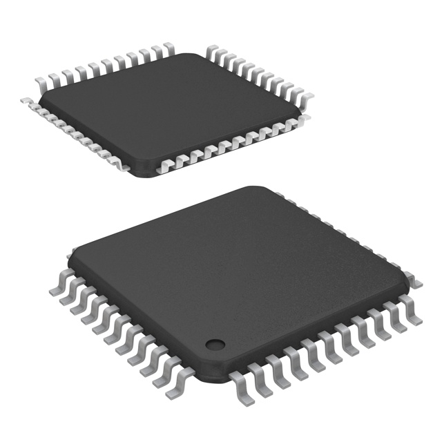
The physical 24-PDIP form factor reflects a design philosophy targeting both ease of prototyping and long-term reliability. Through-hole mounting provides not only mechanical robustness under vibration or thermal cycling but also facilitates rapid board rework and socketed configurations during iterative design validation. In field service, this yields significant uptime advantages, reducing costs associated with re-soldering or specialized handling.
Significant design insight stems from harnessing the full dual-functionality potential of the AD7730BN’s pins. By leveraging programmable input/output assignments and flexible timing, system architects achieve a balance between performance margin and hardware simplicity. In practice, this means realizing lower component counts, streamlined PCB routing, and more scalable designs—ideals central to efficient, serviceable instrumentation platforms.
System integration and signal processing with the AD7730BN
System integration with the AD7730BN leverages a precision architecture tailored for ratiometric signal acquisition, facilitating robust interfacing within advanced measurement, automation, and industrial sensor applications. At the core, the analog front-end chains a low-noise buffer with a programmable gain amplifier, optimizing dynamic range for a variety of transducer outputs. The integrated sigma-delta modulator ensures high linearity by oversampling and noise-shaping low-frequency signals before digital extraction. This structure serves to maximize effective number of bits (ENOB) in environments prone to interference.
The digital signal processing pipeline is differentiated by its user-configurable filtering logic. A cascade of a 22-tap FIR filter and a Sinc3 filter allows precise tailoring of filtering behavior to the system’s temporal response requirements. By toggling skip or fast step response modes, designers can prioritize either transient recovery or steady-state noise suppression, directly matching the sensor’s physical response time and application throughput targets. This modality yields a practical advantage in systems where electromagnetic or mechanical interference profiles shift, such as in multi-range industrial platforms or process automation nodes experiencing variable cycle times.
Critical to maintaining measurement integrity over time, both input and output chopping are implemented to suppress offset errors and thermal drift. These chopping schemes are especially effective at mitigating low-frequency noise and 1/f effects inherent in resistive bridge and capacitive sensors. For low-signal-level measurements—such as precision load cells or medical instrumentation—these features enhance stability and reduce calibration cycles, directly translating to lower long-term maintenance overhead.
Calibration logic, including internal zero and span adjustment as well as external tare compensation, is seamlessly embedded within the conversion pipeline. This enables remote recalibration and compensation routines in distributed systems without incurring downtime or manual intervention, a significant operational benefit in legal-for-trade or safety-critical deployments. Such flexibility supports compliance and extends operational lifespans, even where environmental drift or mechanical stress would otherwise compromise accuracy.
Communication between the AD7730BN and host controllers is optimized via a minimal digital interface compatible with both standard SPI hardware and bit-banged microcontroller IO. The reduced pin count alleviates PCB congestion, ensuring clean routing in high-density designs and simplifying EMC mitigation. This interface strategy underpins rapid prototyping and system scalability, particularly valuable in modular architectures where measurement nodes may be dynamically configured or replaced.
From a practical standpoint, integrating the AD7730BN streamlines the migration from traditional analog signal conditioning—often involving multiple discrete components—towards consolidated mixed-signal front-ends. By embedding both analog performance enhancers and flexible digital filtering, the device enables rapid adaptation to new sensors or evolving measurement regimens. Observed in multi-sensor platforms, the ease of in-field reconfiguration has proven instrumental in reducing system downtime and tuning effort, while the inherent chopping and calibration mechanisms have demonstrated robust drift immunity across extended deployment periods.
Strategically, the AD7730BN’s approach bridges the gap between flexible, software-based digital processing and solid-state analog integrity. Its modular filtering and precision correction features eliminate the calibration bottlenecks common in legacy systems, yet preserve hardware-based noise rejection fundamental to reliable low-level measurement. This balance supports both incremental system upgrades and greenfield smart sensor node deployments, ensuring forward compatibility as measurement fidelity and integration requirements escalate within industrial and test environments.
Power, package, and environmental considerations for the AD7730BN
Ensuring robust and predictable performance of the AD7730BN requires close analysis of the interrelated domains of power, packaging, and environmental robustness. At a foundational level, the analog section mandates a stable AVDD rail between 4.75 V and 5.25 V, narrowly bracketing the nominal 5 V to accommodate low-noise acquisition and minimizing ground loops. On the digital side, DVDD flexibility extends from 2.7 V to 5.25 V, supporting a seamless interface to both 5 V TTL/CMOS and low-voltage digital cores—an adaptability that streamlines system integration, especially when reusing board layouts or retrofitting existing designs.
Supply current behavior underpins thermal and decoupling strategies. The analog domain, manifesting up to 22.3 mA at the rails, requires low-impedance bypass capacitors positioned as close as possible to supply pins. The digital current, scaling from 1.3 mA upwards based on DVDD, reflects data bus activity; careful assignment of ground return paths and the avoidance of shared analog-digital return loops mitigate crosstalk—particularly critical when the modulator operates at near-maximum throughput. During validation, voltage droop under transient load spikes is best managed with a parallel combination of low-ESR ceramic and bulk tantalum capacitors.
Package selection also emerges as a nontrivial contributor to reliability and manufacturability. The 24-lead PDIP, standardized at 0.3" (7.62 mm) width, aligns with legacy through-hole assembly lines, simplifying both prototype rework and field servicing. Critically, the form factor’s respectable thermal impedance enables predictable junction temperature management even where heat dissipation margins are slim. For applications in constrained enclosures or with limited airflow, attention to pad size and copper plane area further augments heat spreading; this approach becomes essential when operating near the documented maximum power dissipation threshold of 450 mW.
Mechanical and electrical protection flows from the device’s absolute maximum ratings. ESD resilience demands careful PCB layout—minimizing trace lengths at analog inputs and employing perimeter ground shields wherever feasible. Absolute limits on supply and I/O voltages warrant input clamp circuits—commonly using Schottky diodes to enhance survivability during handling and power transients. During board-level qualification, controlled humidity and temperature cycling confirm compliance across the specified industrial operating range and mitigate latent failures stemming from micro-cracking or delamination.
Environmental compliance roots itself in both process compatibility and device longevity. The Molded Plastic (PDIP) package’s MSL 1 rating ensures indefinite floor life under standard ambient conditions, reducing constraints during component storage or logistical delays. RoHS compatibility, meanwhile, not only assures legislative adherence but minimizes outgassing during reflow, a critical factor in mission-critical or hermetically sealed equipment. Successful field deployments often couple these behaviors with rigorous board cleaning to eliminate flux residues that could otherwise shift leakage currents and compromise precision analog performance.
Practical experience shows that comprehensive attention to grounding topology, coupled with proactive thermal and EMI analysis, greatly reduces the incidence of subtle performance degradation or latent failures. For high-accuracy instrumentation or safety-related deployments, integrating these design-for-reliability principles early in the schematic and layout process pays substantial dividends in lifecycle stability and regulatory compliance. Adopting this layered strategy, engineers can extract maximum value from the AD7730BN’s flexible power domain, robust package, and industrial-grade resilience.
Potential equivalent/replacement models for the AD7730BN
Selecting an equivalent or replacement for the AD7730BN requires methodical evaluation of both system-level and component-specific parameters. The AD7730L stands out as an immediate candidate due to its shared sigma-delta architecture and functional similarities. However, the alternative’s package options, such as 24-SOIC and 24-TSSOP, demand careful attention. Mechanical compatibility, board layout modifications, and automated assembly processes hinge on such package differences. Additionally, the AD7730L introduces distinct master clock input characteristics; verifying timing margins under the target system’s operating conditions becomes essential to prevent data acquisition errors or communication faults.
Beyond direct descendants within the Analog Devices portfolio, the AD779X and AD778X families encapsulate broader sigma-delta AFE options—offering enhancements in noise performance, input scalability, and digital filter configuration. However, these devices typically diverge in register mapping, supported interface protocols, and feature set. Comprehensive matrix comparison, including pin-level versus system-level signal functionality, informs the extent of required firmware adaptation and hardware respin. Implementing such replacements without granular signal path and timing analysis frequently exposes issues in synchronization, calibration, or thermal drift compensation, especially in precision sensing or industrial measurement applications.
Critical parameters governing replacement feasibility include the supported input ranges, internal programmable gain amplifier resolution, filter flexibility, and digital interface choices. Statistical process control in production environments benefits from maintaining the calibration and noise shaping characteristics associated with the original AD7730BN. When deviations are introduced by new filter structures or reference input schemes present in later-generation parts, adjustment of production test routines and system self-calibration processes may be necessary. Careful simulation of signal integrity—especially under conditions mimicking aging or environmental extremes—guards against unplanned downtime or measurement drift.
Practical integration experience reveals that package migration frequently impacts EMC compliance, especially when transitioning to smaller footprints or revising ground plane strategies. Software compatibility is influenced not only by instruction-level register changes but also by device startup and reset behavior, often overlooked during documentation reviews. Close coordination between procurement, hardware design, and firmware teams accelerates risk mitigation, highlighting any subtle mismatches before committing to volume production runs.
Substitution strategies benefit from prioritizing architectures with proven supply longevity and multi-vendor sourcing options, reducing lifecycle obsolescence risk. Considering pin-compatible drop-in replacements streamlines support for field-replaceable units in legacy instrumentation, while embracing newer models with advanced diagnostics and lower power consumption can future-proof measurement platforms. These choices must balance immediate hardware constraints with longer-term maintainability and system evolution pathways—calling for a disciplined, documentation-driven approach to device selection and qualification.
Conclusion
The Analog Devices AD7730BN analog front end established critical performance standards in high-accuracy sensor signal chains, particularly for weigh-scales and pressure transducers requiring precise and stable digital conversion. At the architectural level, the device integrates a 24-bit sigma-delta ADC with optimized noise coefficients, providing engineers with an exceptionally wide dynamic range for microvolt-level sensing applications. This ADC core is tightly coupled with programmable digital filtering, enabling application-specific tailoring of throughput and rejection of line-frequency interference. The dual differential inputs facilitate ratiometric measurement, eliminating common-mode error sources—a decisive factor in industrial environments prone to electrical noise.
Robust electrical and thermal immunity is achieved through on-chip calibration, input buffering, and adaptive biasing, ensuring stable performance across diverse deployment scenarios. The advanced serial digital interface minimizes PCB complexity while supporting streamlined communication protocols, accelerating integration in multiplexed sensor arrays and distributed acquisition systems. As a result, designers have historically leveraged the AD7730BN’s platform flexibility to balance board space, precision, and long-term maintainability. For instance, engineers transitioning between sensor bridge topologies could dynamically reconfigure channel gain and offset without hardware modifications, preserving rapid prototyping workflows.
With the AD7730BN classified as obsolete, present-day system architects face a nuanced migration path. Substitution analysis must extend beyond simple pin-to-pin replacement; it requires thorough evaluation of timing parameters, filter response characteristics, and analog front-end input impedance, as variance in these domains directly impacts overall measurement fidelity. Additionally, form factor and mechanical compatibility frequently dictate layout adjustments, affecting system EMC and thermals—a reality often overlooked during spec-driven component selection. Detailed examination of supply chain continuity and documentation quality also informs selection of successors, mitigating downstream integration risks.
Modern alternatives increasingly offer higher degree of configurability, integrated calibration algorithms, and enhanced energy efficiency. However, integration densities may introduce unforeseen cross-talk, or higher digital noise if not carefully managed—a trade-off necessitating advanced simulation and validation at the PCB level. In mixed-signal environments, maintaining the noise floor and rejection ratios as established by the AD7730BN often requires a hybrid approach: supplementing advanced ADC chips with dedicated low-noise analog front ends or shielded PCB layout strategies. Direct design reuse of AD7730BN-based modules for legacy support demonstrates an advantage because of the device’s proven stability under field conditions. System-level decisions, therefore, must balance the reliability of established architectures against the functional breadth of next-generation offerings.
Careful examination of characteristic parameters shows the AD7730BN remains a reference-point for evaluating noise performance, filter sharpness, and input versatility in contemporary analog front-end selection. Leveraging disciplined analytical methods, teams can translate these benchmarks into tangible selection criteria for current high-precision sensor acquisition systems, minimizing both integration friction and lifetime cost.