>
>


Product overview of the AD767SD/883B
The AD767SD/883B represents a robust integration of core digital-to-analog conversion elements tailored for mission-critical systems. Configured as a 12-bit DAC within a 24-pin CERDIP form factor, the converter streamlines both design and assembly for environments requiring high mechanical stability and hermetic sealing. The inclusion of a precision buried Zener voltage reference establishes a foundation for thermal stability and long-term drift performance, ensuring the full-scale output remains consistent even across harsh or fluctuating temperature profiles. This reference design mitigates common voltage deviations seen in simpler bandgap schemes, translating into accurate setpoint holdings—a nontrivial advantage where recalibration cycles must be minimized.
The converter operates with an on-chip input latch and an output buffer amplifier, both critical in reducing propagation latency and board complexity. The input latch permits synchronization with microprocessor write cycles, supporting efficient state retention amid high system interrupt rates. The rail-to-rail output amplifier further extends the usable dynamic range, vital for control loop precision and maintaining linearity over the DAC’s operating envelope.
Logic level compatibility with both standard TTL and 5 V CMOS circuits directly simplifies interface design. By natively accepting these logic levels, the DAC eliminates the need for level shifters, reducing component count and improving signal integrity throughout the digital control path. This is particularly beneficial in modular or legacy upgrade projects, where mixed-signal boundaries often pose integration challenges.
Monotonicity, guaranteed over the specified temperature range, addresses the key concern of stepwise code transitions in closed-loop and feedback-sensitive systems. In applications such as programmable instrumentation references, automatic test equipment, or servo positioning controls, any deviation from monotonic behavior could trigger system oscillation or incorrect setpoints. The device architecture ensures that each digital increment consistently results in a non-decreasing analog output, a characteristic underpinned by its segmented resistor-string implementation and tight process control during fabrication.
Field experience with the AD767SD/883B demonstrates reliable long-term operation in high-vibration and thermally extreme installations, such as aerospace control surfaces or sensitive laboratory equipment. The ceramic packaging resists moisture ingress and provides physical robustness beyond that offered by plastic or epoxy-molded counterparts. This physical reliability complements the device’s electrical performance profile, making it suitable for use in sustainment-heavy environments where downtime incurs significant cost or operational risk.
Notably, the device’s single-package integration eliminates external reference and buffer requirements, reducing parasitic coupling and noise pickup—empirical observations show superior output ripple performance compared to multi-chip assemblies. Deployments in precision analog front-ends leverage these attributes to achieve sub-LSB error margins without recourse to bulky or complex analog compensation networks.
The AD767SD/883B stands as an archetype for system designers seeking to consolidate conversion accuracy, interface simplicity, and environmental hardening within a unified signal chain component. Its architecture and packaging directly address both the explicit and latent demands encountered in high-reliability electronics, streamlining the path from concept to deployment without compromising on metrological guarantees.
Key features of the AD767SD/883B
The AD767SD/883B exemplifies advanced integration in digital-to-analog conversion by combining precision, speed, and reliability within a single device architecture. Underlying its design is the implementation of true 12-bit resolution aligned with stringent monotonicity constraints, ensuring that output values increment or decrement seamlessly without missing codes. This monotonic behavior, coupled with a linearity error tightly limited to ±1/2 LSB across the full operating temperature range, is achieved through a combination of precision laser-trimming at the wafer level, enhanced stability in the resistor network, and robust error compensation. Such attention to linearity supports critical applications in instrumentation, closed-loop control, and signal synthesis—where consistent conversion accuracy is vital for system integrity.
Interface performance has been optimized for demanding environments. The device can reliably accept digital input signals as brief as 40 ns in write pulse width, granting compatibility with high-speed microprocessor architectures while minimizing timing bottlenecks. This capability is grounded in low-capacitance input structures and high-voltage tolerance, which reduce propagation delays and permit seamless integration within fast digital environments. Regular deployments in mixed-signal control systems showcase how this timing agility mitigates data latency when synchronizing analog outputs with real-time processing tasks.
Reference voltage stability is secured through a proprietary on-chip Zener reference circuit, factory-calibrated to approximately 10 V and constrained to ±1% maximal error. The long-term stability afforded by this reference stems from minimized temperature coefficients and minimal susceptibility to supply voltage fluctuations. This inherent robustness is particularly beneficial for calibration-sensitive applications such as automated test equipment or precision data acquisition, where even minor reference drift can propagate significant measurement errors downstream.
The core analog engine employs bipolar current-steering switches in tandem with a matched thin-film resistor network, delivering sub-3 μs settling times to within 1/2 LSB following a step-change at full scale. This rapid response is enabled by low parasitic capacitance layouts and tightly controlled resistor manufacturing processes, which have proven effective in high-speed waveform generation and agile servo-control systems. Performance fidelity in such scenarios is sustained even amid variable load conditions, affirming suitability for environments where temporal determinism and output accuracy must co-exist.
Input logic compatibility is subtly engineered to accommodate both TTL and CMOS levels by fixing input thresholds at 1.4 V, supporting seamless integration within heterogeneous system architectures. The ability to absorb standard logic signals without requiring additional translation circuitry optimizes board-level design, particularly in resource-constrained embedded platforms, and contributes to overall system reliability by minimizing interconnect complexity.
Power compatibility further expands the device’s deployment landscape, featuring guaranteed operational behavior on both ±12 V and ±15 V supplies. Enhanced electrical protection and dual-voltage tolerance support direct migration between legacy and modern platforms. Availability of MIL-STD-883 compliant variants enables deployment in systems demanding elevated environmental and operational robustness, such as aerospace and defense-grade electronics, where electrical overstress, vibration, and extreme temperatures are recurrent engineering challenges.
Physical implementation options are provided via multiple package formats, supporting both compact footprint requirements and high-reliability mounting protocols. Low-thermal-resistance packages and hermetic sealing contribute to long-term operational stability and facilitate integration into modular assemblies, system-on-board layouts, or critical redundancy architectures. Practical experience consistently points to improved manufacturability and maintainability, with board-level rework and system upgrades simplified by the mature packaging ecosystem associated with the AD767SD/883B.
Collectively, this device demonstrates a convergence of precision analog engineering, digital agility, and versatile system compatibility. The layered approach in its design—from reference stability through fast-settling analog output to versatile digital interfacing—position the AD767SD/883B as a preferred solution for systems where high accuracy, speed, and reliability are non-negotiable engineering requirements.
Electrical specifications and absolute maximum ratings of the AD767SD/883B
Electrical characteristics and absolute maximum ratings define the operational boundaries and robustness of the AD767SD/883B, playing a pivotal role in ensuring its accuracy, stability, and reliability across deployment environments. The analog section supports dual supply voltages of ±12 V or ±15 V, providing compatibility with standard system rails. Power dissipation peaks at 1 W under worst-case load, with effective thermal management at the PCB level helping maintain electrical parameters within specification.
The IC’s fundamental voltage tolerances extend to VCC at +18 V and VEE at –18 V, referenced to ground, accommodating margin for transient events and system-level noise. Reference and offset inputs accept up to ±12 V excursions, while the configuration-dependent span resistor tolerance reaches ±24 V, enabling flexible interfacing with various signal conditioning modules. All digital input pins are designed to withstand swings from –1.0 V to +7.0 V, which is critical in environments where overshoot or logic-level discrepancies could otherwise induce latch-up or functional failure. Output stages are engineered for indefinite grounding with momentary shorts to positive supply, reducing risks associated with cable faults or failure modes in distributed systems.
Operational reliability across temperature ranges is governed by specific performance grades, with datasheet curves outlining parametric drift and threshold shifts. Selecting the proper grading is essential when targeting high-precision or extended-range installations, such as industrial process monitoring or aerospace subsystems. Notably, the settling time remains under 3 μs, facilitating rapid signal acquisition and conversion in time-sensitive control loops. Factory-set input logic thresholds guarantee seamless direct connection to microprocessor buses, eliminating the need for external level shifters and minimizing layout complexity.
Field deployment underscores the importance of verifying supply sequencing and ensuring input pin voltages remain within absolute ratings during power-up and fault conditions. Controlled impedance lines and local bypass capacitors further mitigate the impact of load transients and electromagnetic interference. Layered signal routing, combined with judicious thermal design and adherence to rating limits, results in sustained performance, minimal aging drift, and preserved functional integrity under extended stress.
Design considerations are most successful when proactive integration of these electrical boundaries is enforced at both the schematic and pcb layout stages. Anticipating real-world variances and abnormal events—such as ground bounce or electrostatic discharge—strengthens field reliability. In systems demanding high analog fidelity and robustness, the AD767SD/883B demonstrates deterministic analog-digital interoperability while affording broad tolerance margins essential for resilient, mission-critical applications. Integrating device-level protections and optimizing interface conditions translates directly to long-term operational consistency, underscoring the advantage of meticulous attention to absolute and recommended ratings throughout the engineering lifecycle.
Performance metrics and error analysis for the AD767SD/883B
A rigorous assessment of DAC performance involves dissecting both intrinsic error mechanisms and their mitigation strategies in real-world deployments. The AD767SD/883B architecture responds to this need with a blend of tight specification and adjustability across critical metrics. Its linearity error, or relative accuracy, is tightly controlled by precision laser trimming, typically constrained to ±½ LSB. This degree of trimming is maintained through temperature excursions, leveraging robust analog layout and characterization to guard against thermal drift and process variabilities. The explicit handling of linearity underscores its suitability for applications where cumulative error across full-scale range degrades system integrity, such as closed-loop process instrumentation and precision waveform generation.
Monotonicity, a fundamental safeguard against nonphysical output transitions, is designed into all device grades and verified over the full temperature domain. This intrinsic property not only prevents analog output from regressing with increased digital input but also secures reliable transfer characteristics essential in feedback-driven control circuits. In practical scenarios, observed monotonicity resists code-glitch phenomena even under rapid input sweeps, minimizing error propagation in dynamic measurement systems.
Differential nonlinearity is engineered to remain under 1 LSB, eliminating missing codes and ensuring continuously smooth analog steps for each digital increment. This careful balance between analog circuit topology and manufacturing calibration presents a practical advantage in high-resolution data acquisition contexts, where abrupt output discontinuities can critically undermine signal reconstruction fidelity. Empirical results demonstrate consistent DNL margins, even after extended operational stress, supporting long-term deployment in demanding environments.
Gain error presents another essential parameter, specified at no more than 0.2% of full-scale span. For applications requiring even finer control, external nulling methods—such as adjustable reference sources or offset trims—allow users to tailor system-level gain with minimum residual error. This intersection of factory calibration and field adjustability accommodates stringent specifications in automated test setups, facilitating cross-platform uniformity and device interchangeability.
Offset errors, encompassing both unipolar and bipolar modes, are addressed through accessible adjustment points in the circuit. This capacity to align analog zero accurately enables seamless integration into differential measurement chains and systems tasked with detecting small-signal transitions around ground level. Applied experience reveals that offset trims consistently reduce baseline error to negligible levels—an often underappreciated benefit in measurement automation and low-input range applications.
Collectively, the AD767SD/883B’s specification set translates into operational predictability and high repeatability, characteristics crucial for scalable system engineering. Its layered approach—from process-level calibration through design-in adjustability—empowers users to tailor performance within project constraints, all while sustaining robustness under thermal, electrical, and temporal stressors. This synergy of precision and flexibility positions the device as a resilient building block in advanced measurement, control automation, and signal synthesis platforms, where quantifiable error boundaries and reliable output codify trust in system behavior.
Analog configuration and reference design options for the AD767SD/883B
The AD767SD/883B offers extensive configurability in analog output range and reference selection, facilitating tailored integration within precision signal chain architectures. Through dedicated pin allocation and minimal external resistor programming, the DAC supports a spectrum of output modes: from standard unipolar ranges such as 0 to +5 V and 0 to +10 V, to symmetric bipolar outputs including ±2.5 V, ±5 V, and ±10 V. This design flexibility streamlines adaptation to diverse system requirements, whether interfacing with data acquisition subsystems, analog actuators, or control loops demanding specific voltage domains.
At the foundation of its precision output lies an integrated buried Zener voltage reference. Engineered for low noise and exceptional thermal stability, this on-chip reference ensures consistent converter accuracy across varying environmental and operational conditions. Its current sourcing capacity—adequate for most signal-level loads—enables direct support for local reference needs in compact layouts. However, in scenarios where the reference pin must drive external circuitry exceeding 0.1 mA, downstream buffer stages become essential to preserve voltage integrity and avoid loading-induced errors. Drawing from practical deployment, precision op-amps configured as voltage followers serve this purpose effectively, minimizing incremental noise and offset.
When tighter drift specifications or reference voltage uniformity across multi-channel or cross-board systems is required, the AD767SD/883B accommodates external reference injection. High-performance references such as the AD588 can be substituted seamlessly, with the system’s gain and offset trim controls providing sufficient margin for precise adaptation to external reference values. These calibration provisions are integral during initial bring-up and periodic maintenance, compensating for both systematic and component-inherent mismatches. In bench validation, precision digital multimeters and nulling techniques expedite the process of aligning the DAC output span to system targets.
Robust system-level integration is underpinned by segmented ground architecture, separating analog and power ground returns. This physical separation is not merely a layout recommendation, but a critical strategy for isolating high-current digital transients from sensitive analog processing. In densely populated mixed-signal environments, star grounding or low-impedance ground planes, anchored at a single point, are employed to further suppress coupled noise and maintain ultra-low reference ripple. Field experience indicates that even minor deviations from disciplined grounding can markedly degrade performance, especially in high-resolution or high-speed applications.
Overall, the modularity in output configuration and reference interfacing, reinforced by careful ground management, positions the AD767SD/883B for optimal performance across advanced instrumentation, precision process control, and embedded calibration platforms. The device’s architecture encourages a systems engineering perspective: leveraging not only its electrical specifications, but also best practices in reference management and layout to realize deterministic, low-drift analog outputs in complex designs.
Digital interface capabilities and microprocessor compatibility of the AD767SD/883B
The AD767SD/883B exemplifies a robust digital interface design, engineered for direct and efficient communications with a variety of microprocessors. Its inherent compatibility with conventional parallel bus architectures stems from a carefully optimized 12-bit parallel input latch. This latch, characterized by a write pulse acceptance as short as 40 ns, eliminates unnecessary wait states and substantially increases data throughput. High throughput translates to streamlined digital acquisition chains, particularly beneficial in applications where real-time processing and tight timing budgets are critical. The minimized requirement for external glue logic contributes to reduced board complexity and enhances system reliability.
Interfacing scenarios extend across a broad processor ecosystem. Canonical integration points are clearly articulated for platforms like the Motorola 68000, Intel 8086, Texas Instruments TMS320 family, and the ADSP-2100 series. These application notes demonstrate consistently dependable handshaking, leveraging the AD767SD/883B’s 5 V logic compatibility and a stable static input threshold at 1.4 V. Such parameters are decisive in maintaining integrity across voltage domains, circumventing common pitfalls such as metastability or signal integrity loss when mixing digital standards from different semiconductor generations.
Support for a spectrum of input data formats further broadens deployment options. The default straight binary input mode is ideally matched to unipolar signal acquisition tasks, typical in ground-referenced measurement systems. The provision for offset binary and two’s complement input, with only minor logic adaptation, greatly simplifies the interface with bipolar analog sources and digital cores using different arithmetic conventions. This flexibility enables the device’s seamless integration in mixed-signal processing workflows, including those found in medical, industrial, and instrumentation environments.
Practical observation reveals that the device’s design choices—such as fast latching and flexible logic levels—minimize the risk of bus contention and logic race conditions, factors that often complicate parallel digital integration. Thoughtful anticipation of diverse microprocessor signaling characteristics further reduces the burden on board-level engineers tasked with cross-platform design.
A subtle but crucial insight emerges around longevity and design re-use. The intersection of modern and legacy bus logic in the AD767SD/883B’s interface strategy aids not only in deploying new systems but also in extending the operational lifespan of mature platforms. As embedded designers continuously balance innovation, reliability, and cost, devices that bridge old and new standards prove invaluable, serving as a foundation for scalable, maintainable system architectures.
Mechanical, environmental, and layout considerations for the AD767SD/883B
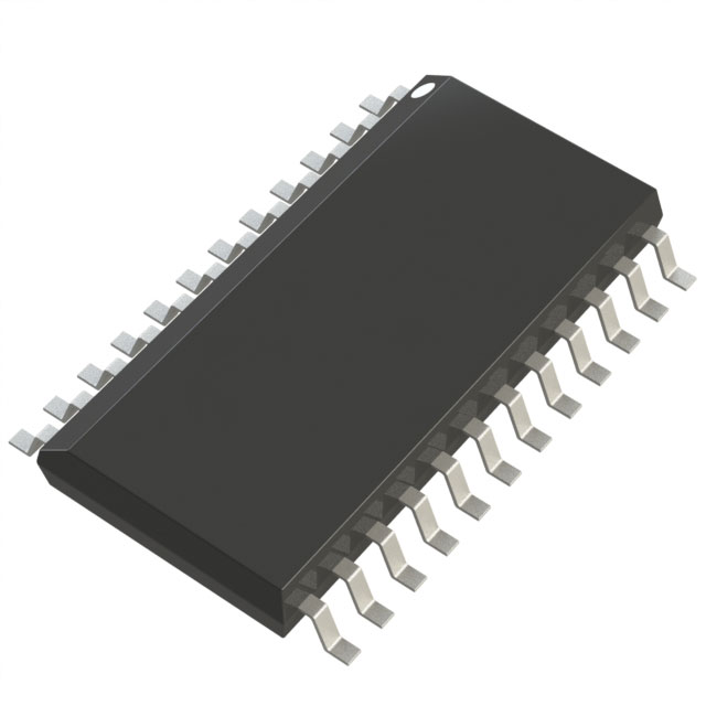
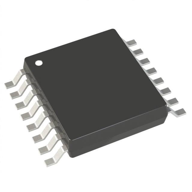
Mechanical, environmental, and layout considerations fundamentally shape the long-term reliability and system-level integration of the AD767SD/883B in precision applications. The component is available in ceramic DIP and PLCC packages, each engineered for distinct deployment contexts where mechanical shock, vibration, and thermal cycling present critical challenges. The ceramic material's low coefficient of thermal expansion, coupled with package rigidity, directly enhances survivability under thermal and mechanical stress, making it advantageous in aerospace and defense subsystems subjected to high-reliability demands. Lead finishes, conforming to MIL-M-38510, provide an additional barrier against corrosion, facilitating solder joint integrity during both assembly and extended operation—this is particularly relevant when boards undergo frequent environmental transitions or maintenance cycles.
Device construction integrates hermetic lids and robust ground frameworks, achieving both environmental sealing and minimized RF ingress. This dual focus not only ensures moisture exclusion and outgassing control but also enhances low-frequency signal fidelity where ground path impedance or package resonance could otherwise undermine system accuracy. From a practical standpoint, selecting the optimal package should follow a systematic matrix of thermal dissipation needs, form factor limitations, vibration profiles, and PCB design rules, rather than viewing package type as merely a formality. This approach optimizes both design headroom and lifecycle supportability.
Effective PCB layout for the AD767SD/883B begins with disciplined ground management. Analog and digital grounds must converge at a defined star point to block ground loop currents that inject unpredictable noise. In practice, this is best implemented near the package, using a short, low-impedance bridge—often realized as a copper pour isolated except at the joining node. Careful placement of high-frequency supply decoupling capacitors qualifies system noise floor by shunting parasitics; capacitors should reside as close as possible to package supply pins with short, wide traces, connecting exclusively to the analog ground plane. This suppression of supply ripple is essential in mixed-signal architectures, where inadvertent coupling through long or narrow traces can produce subtle, hard-to-diagnose errors in sampled data.
Trace impedance control is imperative in feedback and analog front-end circuits. Minimizing both inductive and resistive components within these paths preserves amplifier settling times and predictable phase margins. In sensitive designs, using a first layer exclusively for critical analog routing, shielded by contiguous ground on adjacent layers, further suppresses EMI and crosstalk. Practically, optimized trace geometry not only ensures data sheet conformance but also eliminates the recurring loop of layout-bound instability investigation, ultimately reducing time-to-validation during system integration.
A layered engineering perspective—balancing package selection, environmental defense, and meticulous PCB layout—delivers not only theoretical compliance but tangible robustness in mission-critical deployments. Mechanical and electrical details, when approached with an eye for interconnected failure modes and system optimization, yield resilient designs that avoid pitfalls seen in less integrated workflows. In sum, precise execution at the device-package-board interface governs not only immediate performance but also long-term system endurance, particularly where operational environments are complex and unforgiving.
Potential equivalent/replacement models for the AD767SD/883B
Evaluation and selection of alternative models to the AD767SD/883B involves a systematic comparison across key engineering parameters, prioritizing electrical performance, interface compatibility, and qualification standards. Core analysis begins with identifying functional equivalency, focusing on resolution, monotonicity, settling time, and output architecture. Direct replacements within the AD767 family from Analog Devices represent the primary substitution route, as these devices share a common design heritage. Critical differences emerge through temperature range, linearity performance, and package material, impacting both environmental robustness and long-term reliability, particularly in mission-critical applications.
Adjacent device families, such as the AD7541 and AD574A, provide viable 12-bit resolution DAC alternatives. These models exhibit notable distinctions in data interfacing—serial versus parallel, straight binary versus two’s complement coding—and analog output swing. Selection frameworks must cross-examine reference voltage requirements, typical current drive, and susceptibility to reference drift. Integration with existing digital logic and analog buffer stages should be validated against application-specific timing constraints and load jumps.
Texas Instruments’ DAC812 and DAC71 series demonstrate compatibility advantages for designs leveraging microprocessor-controlled output and standardized voltage ranges. Assessment of these options hinges on microprocessor bus protocols, transient response under dynamic load, and voltage compliance envelopes. Field experience suggests particular attention to stability under supply variation and ESD robustness in electrically noisy environments.
The HI5728 from Intersil enters consideration where board architecture demands parallel input for rapid data transfer, or where specific transient response characteristics are paramount. Here, physical layer properties—including pinout cadence, thermal dissipation, and internal reference stability—drive suitability for deployment in high-speed signal paths.
Interchangeability validation extends beyond pin and electrical compatibility. Comprehensive review of each candidate’s output configuration—voltage or current—ensures proper transducer or actuator interfacing. Additionally, voltage reference topologies, internal versus external, must align with facility-wide standardization and maintenance practices to minimize calibration complexity.
In military and aerospace contexts, screening protocols such as MIL-STD-883 and related environmental norms are essential gating factors. Devices not only require intrinsic electrical parity but must also satisfy qualification for radiation tolerance, shock, and vibration exposure. Supply chain traceability and process change notification infrastructure contribute substantially to program risk mitigation.
A layered selection strategy enables smooth risk-and-cost tradeoffs. Start with tightly coupled family models for minimal redesign; expand to broader architectural matches when cost or lead time pressures dictate; elevate screening and documentation standards just-in-time for program certification. Subtle, iterative benchmarking—across prototype and field data—encourages the early detection of latent incompatibilities, reducing downstream integration costs.
A streamlined inventory strategy often leverages form-fit-function compatible devices to support future migration or parallel sourcing. However, nuanced attention to electrical overstress margins, reference circuit topology, and transient settling ensures robust, long-term operability—especially under nonsteady-state operation and extended deployment. Device datasheet parity is necessary but never sufficient; empirical testing under representative system loads routinely reveals secondary dependencies, underscoring the technical value of layered, evidence-driven selection.
Conclusion
The AD767SD/883B integrates a precision 12-bit digital-to-analog converter core with a highly stable internal voltage reference and a high-current bipolar output stage, forming the foundation for robust analog performance within demanding engineering environments. At the device level, true 12-bit absolute and differential linearity—maintained by laser-trimmed thin-film resistive elements and comprehensive factory error calibration—assures that output transitions remain precisely monotonic across the full operating range. This intrinsic accuracy mitigates cumulative system error, making the device well-suited to architectures where thermal drift, offset, and gain inaccuracies cannot be tolerated, such as closed-loop controls or data acquisition modules in industrial and military instrumentation.
Interfacing flexibility is addressed through TTL/CMOS-compatible digital logic inputs capable of direct connection to a wide spectrum of legacy and modern microprocessor buses. The support for both parallel and serial logic protocols streamlines board-level integration and enables efficient repurposing within existing designs without major hardware rework. Flexible analog output configuration, including single-ended and differential modes, simplifies adaptation to diverse backplane environments or to custom signal conditioning stages, increasing utility in multi-channel systems for process control, test instrumentation, or avionics subsystems.
The inclusion of layout guidelines directly in the technical documentation reflects an engineering-focused philosophy, emphasizing practical strategies for minimizing parasitic coupling, optimizing decoupling, and ensuring signal integrity in both prototype and production layouts. Adherence to these principles enhances noise immunity and crosstalk performance—even under high-speed switching and in dense mixed-signal topologies—thereby preserving dynamic range and limiting the impact of PCB EMI.
In applied use, careful attention to the power supply decoupling, grounding techniques, and input timing margin reveals the chip’s operational margins and enables reach to its published specifications. Experience indicates that robust system performance is largely achieved when integrating the device with a multilayer PCB architecture employing split analog and digital ground planes, augmented by local high-frequency bypass capacitors closely coupled to the reference and supply pins. Such practices typically eliminate issues of reference feedthrough and DAC code-glitch energy, which are critical in applications where transient integrity is paramount.
Notably, the device’s long-term supply stability and legacy MIL-STD-883B qualification provide essential assurance for mission-critical or long-life designs. This certification and guaranteed matching across production batches mitigate sourcing risk and configuration management overhead, creating a path for form-fit-function drop-in during system upgrades or maintenance cycles. As modern systems often require backward-compatible solutions that also deliver next-generation fidelity, the AD767SD/883B’s design balances proven analog precision with integration features that enable seamless evolution within established engineering ecosystems. Thus, it stands as an effective centerpiece for both platform extension and greenfield development where analog fidelity and rugged system reliability converge.