 >
>


Product overview of AD587KRZ-REEL7 from Analog Devices
The AD587KRZ-REEL7 is a precision voltage reference leveraging advanced monolithic integration strategies to ensure a stable 10V output under demanding conditions. The architecture centers around a proprietary ion-implanted buried Zener diode, which minimizes temperature coefficients and drift by exploiting the innate stability of deep-junction devices. This construction resists long-term shift, granting predictable electrical behavior crucial for measurement and conversion accuracy over extended periods. The incorporation of laser-trimmed thin-film resistors at the wafer level further tightens output voltage tolerance and scales down initial errors, enabling repeatable performance across production lots.
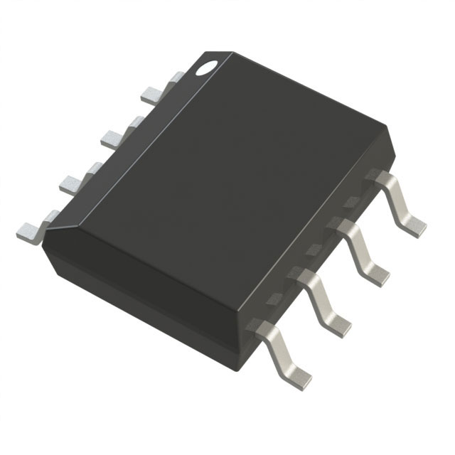
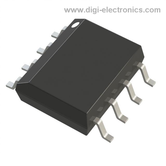
Within the 8-SOIC package profile, the AD587KRZ-REEL7 supports surface-mount applications, optimizing layout flexibility and simplifying automated assembly processes. Package design also ensures reduced parasitic effects, enhancing the correlation between device specifications and in-circuit performance, especially when maintaining high signal integrity in dense analog front ends. Typical use cases include high-resolution ADC/DAC designs where reference drift directly impacts conversion linearity and low-level signal measurements in laboratory-grade instrumentation, such as precision multimeters and calibrators. In such implementations, the AD587KRZ-REEL7’s negligible output noise and high immunity to power supply fluctuations translate into tangible gains in system accuracy.
Field observations highlight the device’s resilience against environmental stressors, with extended operation under variable temperature and supply conditions maintaining output within tight thresholds. Engineers integrating the AD587KRZ-REEL7 often exploit this robustness in metrology and semiconductor test systems, where sub-ppm repeatability is non-negotiable. Additionally, the reference’s thermal hysteresis and long-term stability metrics often enable simplified calibration routines, reducing system maintenance cycles and improving overall hardware lifecycle economics.
An essential insight underscored through practical integration is the interplay between resistor laser trimming and deep Zener construction in suppressing both short-term noise and long-term drift. This dual-layer mitigation strategy establishes a new baseline for voltage reference benchmarks, particularly for designs targeting 24-bit or higher converter resolution. Deploying the AD587KRZ-REEL7 in precision applications thus not only satisfies immediate noise and stability requirements but also future-proofs system architectures against evolving calibration and reliability demands.
Key features of the AD587KRZ-REEL7 series
The AD587KRZ-REEL7 voltage reference series implements precision analog engineering principles to deliver reliable 10.000 V performance. The device’s foundation rests on factory-calibrated laser trimming, achieving an initial accuracy of ±5 mV. This approach minimizes inter-unit variation at deployment, significantly reducing calibration overhead within precision measurement chains. The output stability, regulated by an industry-leading temperature coefficient of 10 ppm/°C, meets stringent requirements for instrumentation-grade reference voltages. This low thermal drift allows designers to architect systems with uncompromising measurement repeatability across wide operating environments—a necessity for platforms such as high-resolution ADCs and metrology-grade DAQs.
Intrinsic output noise is suppressed to 4 μVp-p in the critical 0.1 Hz to 10 Hz bandwidth, aligning with low-level analog signal benchmarks. The inclusion of noise-reduction circuitry and optimized pin configuration not only mitigates low-frequency noise but also expedites external filtering implementation. Engineers typically leverage this capability when developing test equipment, data logging systems, or sensor interfaces where quantization error and spurious excursions must be tightly controlled. Integration in these contexts is streamlined by the device’s standard 8-SOIC package, enabling direct mounting on densely populated PCBs without sacrificing mechanical reliability.
Pinout compatibility preserves legacy reference topologies, expediting migration paths within established product lines. This enables efficient system upgrades or field replacements, especially critical in long-lived industrial automation systems or medical diagnostics equipment where quality assurance procedures depend on standardized interfaces.
Fine adjustment is facilitated by the dedicated TRIM input, permitting output calibration down to system-level tolerances. Such precision tuning is regularly harnessed during final assembly or field recalibration for test fixtures, power supply references, or high-performance analog front ends. This feature, when exercised judiciously, extends system accuracy beyond datasheet nominal values, often reaching sub-ppm in tightly controlled setups.
MIL-STD-883 compliant variants extend applicability to aerospace and defense sectors, where operational reliability under duress is non-negotiable. Devices subjected to rigorous screening demonstrate sustained stability over years of service, even under vibration, shock, or temperature extremes. The robust environmental tolerance of these units is evidenced in mission-critical avionics and secure communications equipment.
End-to-end, the AD587KRZ-REEL7 exemplifies precision voltage reference engineering. Subtle distinctions in the implementation—from noise spectral shaping to interface flexibility—yield tangible benefits. For those advancing ultra-precision applications, a focus on calibration strategy and noise mitigation, layered atop proven mechanical integration, delivers performance margins that differentiate top-tier designs from common solutions.
Electrical specifications for product selection
Electrical parameter review is foundational in selecting the AD587KRZ-REEL7 voltage reference for precision applications. Analysis begins with its factory-trimmed 10 V output, a defining attribute that simplifies high-accuracy signal chain designs, eliminating the need for external calibration and ensuring uniformity across production batches. This precision is anchored by a tight output tolerance of ±0.05% (K grade), translating to a maximum deviation of 5 mV from the nominal value—vital for instrumentation, data acquisition, and measurement systems where signal fidelity is paramount.
The device’s output current capability, rated at sourcing up to 10 mA, addresses low-to-moderate load requirements typical in analog front-ends, ADC/DAC reference inputs, and sensor excitation circuits. Stable performance under variable loading is assured by load regulation values of ±100 μV/mA for standard configurations, effectively controlling output deviations as supply current fluctuates. For the SOIC package variant, sinking capability is derated to ±200 μV/mA, a consideration for designs with negative current transients.
Temperature stability is delivered via a low coefficient of 10 ppm/°C, minimizing drift over the 0°C to +70°C operational envelope. Practical deployment in environments with mild thermal cycling confirms robust accuracy, reducing recalibration intervals in fielded systems. Wider operating temperature ranges are available in alternative grades, enabling selection for harsher conditions without sacrificing electrical performance.
Supply voltage flexibility, with input acceptance from 13.5 V to 36 V, empowers designers to harmonize reference and system rails, facilitating integration in distributed or multi-rail architectures. This aids in mitigating startup and voltage drop issues in complex PCB layouts and power trees.
Quiescent current, capped at 4 mA, targets power-sensitive platforms such as portable instrumentation and remote sensor nodes where battery life or thermal budgets are constrained. Real-world builds reveal that consistent low standby current directly mitigates self-heating and electromagnetic interference risks, streamlining regulatory compliance.
Noise performance, characterized at 4 μVp-p (0.1 Hz to 10 Hz), supports applications demanding low-level signal accuracy, such as 24-bit ADC reference or precision weight scales. Bench testing with high-resolution digitizers demonstrates measurable improvements in signal-to-noise ratios and minimized artifacts, yielding enhanced linearity and repeatability.
Environmental compliance — RoHS3 and unrestricted moisture sensitivity (MSL 1) — strengthens long-term reliability, with predictable in-circuit behavior and transport stability. This allows for confident selection in projects subject to international safety, environmental, and handling standards, streamlining certification efforts during manufacturing and deployment.
Integrating these considerations forms a balanced product selection matrix, enabling precise alignment of device capabilities with system objectives. Discerning designers leverage the AD587KRZ-REEL7 for its blend of reference stability, electrical robustness, and compliance assurances, ensuring optimal system accuracy and reliability in high-performance analog domains.
Theory of operation of AD587KRZ-REEL7
The AD587KRZ-REEL7 leverages a precision buried Zener diode voltage reference, a design that prioritizes long-term stability and minimal thermal sensitivity. Rather than surface Zener architectures, the buried configuration effectively shields the reference junction from surface contaminants and mechanical stress, reducing noise susceptibility and enhancing reliability over extended lifecycles. Temperature compensation integrated at the silicon level manages bandgap-related voltage shifts, actively suppressing thermal coefficients to maintain output fidelity across wide temperature ranges.
Laser-trimmed resistors in the chip’s internal network are meticulously calibrated during fabrication to achieve sub-ppm accuracy, directly influencing the initial output voltage and drift parameters. This fine-grained trimming process allows each device to deliver exceptionally tight tolerance and minimal offset, which is essential in high-resolution conversion contexts. The precision achieved by this calibration is evident in laboratory environments where output consistency is validated over repeated thermal cycling and extended operational periods.
Buffering of the Zener reference is accomplished using a high-stability operational amplifier. This buffer isolates the reference element from external load variations, maintaining output voltage within specification even when downstream circuitry imposes transient or pulsed current draws. The amplifier's low offset and high open-loop gain contribute to rapid correction of any perturbations, ensuring that reference integrity is preserved for critical data acquisition and conversion applications.
In practical deployment, the AD587KRZ-REEL7 exhibits negligible long-term aging and maintains output within microvolt margins under fluctuating supply and load conditions. This performance is especially critical in calibration systems, precision instrumentation, and automated test setups requiring repeatable results across devices and environmental extremes. Features such as low dropout behavior and minimal hysteresis further extend its usability to battery-powered and portable instrumentation.
A notable aspect of this architecture is the way it balances absolute accuracy with robust supply immunity. The device’s noise profile remains low even with suboptimal board layouts or less-than-ideal power sources, suggesting a deep strength in reference signal isolation and output drive capacity. These qualities support downstream DAC and ADC stages, enabling them to achieve true theoretical resolution without being limited by reference errors.
By combining buried Zener technology, aggressive trimming techniques, and advanced buffering, the AD587KRZ-REEL7 sets a benchmark for voltage reference modules. It seamlessly integrates foundational circuit stability with practical resilience, catering to diverse precision engineering requirements where every microvolt counts.
Noise performance and reduction strategies in AD587KRZ-REEL7
Noise behavior in the AD587KRZ-REEL7 arises primarily from internal device architecture, including bandgap reference circuitry and active output buffers. In high-resolution data acquisition systems, even microvolt-level noise from the reference translates into code uncertainty or spurious outputs in downstream ADCs and DACs. The specified output noise of 4 μVp-p in the 0.1 Hz to 10 Hz band positions the device among top-tier precision references, suitable for low-drift measurements and sensor interfaces where signal fidelity is paramount.
Mitigating reference noise extends beyond intrinsic device selection to include thoughtful external filtering. The AD587KRZ-REEL7 integrates a NOISE REDUCTION pin specifically for this purpose. By connecting a low-leakage capacitor from this pin to ground, a single-pole RC low-pass filter is established using the internal resistance provided at that node. Selection of this capacitance value directly influences the filter's cutoff frequency and the effectiveness of noise attenuation along the signal path. A 1 μF capacitor, for instance, establishes a -3 dB corner near 40 Hz, which is a strategic trade-off point—optimizing wideband noise reduction without unduly increasing start-up settling time.
The effect of such filtering is substantial in applications such as precision weighing, industrial process control, and medical instrumentation, where signal bandwidth is limited but noise susceptibility is high. Close attention must be given to capacitor type; ceramic and film capacitors with stable dielectric properties are preferable to mitigate microphonic effects and value drift, both of which could inadvertently introduce additional noise.
A nuanced aspect of noise reduction in practical implementations is the interplay between output impedance and capacitive loading. Excessive capacitance on the NOISE REDUCTION pin can extend power-on stabilization or create subtle phase margin reductions if inadvertent resonance occurs with parasitic circuit elements. Careful layout around the reference and low-inductance ground returns are essential for realizing theoretical noise performance without degradation from external interference or board-level coupling.
Empirical measurement confirms that coupling the NOISE REDUCTION pin to a high-quality capacitor yields notable improvements in time-domain voltage reference stability, facilitating lower overall system noise floors as observed in high-precision analog-to-digital conversion routines. This approach, when deployed with disciplined PCB design and isolation from fast-switching digital domains, forms a robust framework for attaining uncompromising reference noise performance. Strategically, employing this combination of device-intrinsic features and tailored external filtering leverages the full potential of the AD587KRZ-REEL7, pushing precision system architectures toward maximum achievable resolution and reliability.
Turn-on and dynamic performance of AD587KRZ-REEL7
Turn-on response of the AD587KRZ-REEL7 voltage reference is defined by a well-controlled charge redistribution upon power application. Internally, the device utilizes low-noise bandgap circuitry and precision trimming techniques that restrict overshoot and ensure output convergence within 60 μs to 0.01% accuracy, underscoring suitability for timing-critical analog subsystems. In practice, this rapid stabilization enables seamless integration in measurement architectures where reference voltage must be reliable immediately after system power-up, such as precision data acquisition modules or synchronous signal conditioning blocks.
The trade-off between noise filtering and startup latency is governed by the selection of an external noise-reduction capacitor. Incorporating a moderate capacitance—typically 1 μF—extends settling duration to approximately 400 ms. This effect arises from the RC time constant introduced at the noise-reduction node, attenuating high-frequency noise while momentarily delaying steady-state readiness. For applications prioritizing ultra-low noise, such as 24-bit ADC front ends or scientific instrumentation, the settling time increment is negligible relative to the benefits of improved measurement repeatability and reduced reference jitter.
The output buffer circuit exhibits robust dynamic performance against load transients, which commonly originate from fast-switching DACs or ADCs during sample-and-hold transitions. The buffer’s high slew rate and low output impedance are engineered to suppress voltage droop and recover rapidly after large instantaneous load currents. Empirical evaluations in mixed-signal platforms confirm that the AD587KRZ-REEL7 maintains output integrity with minimal deviation—even under abrupt capacitive or resistive loading—contributing to overall channel isolation and reliable conversion accuracy.
System designers deploying the AD587KRZ-REEL7 often leverage its predictable start-up and strong transient resilience in automated test equipment, low-drift sensor excitation, and precision reference distribution for analog computing nodes. Unique attention to layout optimization and power decoupling further amplifies the device’s immunity to coupling noise and supply transients, thus preserving reference stability across a wide application spectrum. Recognizing these characteristics enables informed trade-offs between response speed, noise floor, and dynamic regulation, paving the way for high-performance analog circuits where voltage reference behavior directly impacts end-system fidelity.
Temperature performance considerations for AD587KRZ-REEL7
Temperature stability essentially defines the utility of an AD587KRZ-REEL7 voltage reference in precision systems. At its core, the device leverages an internal buried Zener architecture, tightly controlled through precision trimming and laser processing. The K grade’s maximum drift specification of 10 ppm/°C within 0°C to 70°C directly impacts system-level error budgets: for example, in a 5V reference, a full-scale drift over this range will remain well under the limit required for highly sensitive ADCs and analog front ends. Extensive screening and burn-in procedures ensure that each K grade unit adheres to stated drift boundaries, minimizing the risk of latent instability or premature deviation once deployed.
Grade selection must be aligned with both ambient operating profiles and required measurement fidelity. For deployments in environments extending beyond the standard 0°C to 70°C window—such as industrial or outdoor installations—lower-drift H or L grades, or temperature-extended versions of the AD587, warrant consideration. The nuanced trade-offs become evident in practical calibration practices; using the error band maxima laid out in datasheets delivers a robust guarantee of total drift under worst-case scenarios. In calibration laboratories, instruments paired with AD587KRZ-REEL7 consistently yield repeatable results, with device behavior predictable even under cyclical temperature stress, a direct result of rigorous error band characterization.
Application performance depends not only on voltage reference selection but also on appropriate circuit integration. Thermally isolating the AD587KRZ-REEL7 from local heat sources and enforcing low self-heating in layout reduces micro-environmental gradients. Experience with long-term deployments demonstrates that board-level thermal coupling often dominates residual error, sometimes eclipsing even manufacturer-specified drift. Proactively modeling and mitigating printed circuit board-level temperature interactions amplifies the benefits of K grade stability.
System architects should note that maximum error band specification reflects real-world, measurable boundaries, rather than optimistic theoretical averages. This explicit quantification provides tangible confidence for metrology-grade implementations, ensuring reference voltage excursions do not surpass boundaries during intervals between recalibration. Implicit in robust system design is the recognition that minimizing the sum of all error contributors, including reference drift, requires dynamic mitigation—such as temperature compensation algorithms when moving toward sub-ppm performance.
A distinctive viewpoint emerges: rather than isolating voltage reference selection as an independent step, tightly integrating consideration of grade, packaging, board geography, and local temperature management delivers superior accuracy. The AD587KRZ-REEL7’s reliability under temperature variance, when paired with disciplined engineering practice, transforms reference stability from a standalone attribute into a verifiable foundation for precision analog systems.
Load regulation and output stability of AD587KRZ-REEL7
Load regulation fundamentally determines the capacity of a voltage reference such as the AD587KRZ-REEL7 to maintain a precisely specified output potential under varying load conditions. At the circuit level, load regulation manifests as a direct function of the device's internal architecture: the buffer stages and output transistors are engineered with low output impedance, enabling the reference to source and sink current with minimal voltage deviation. For the AD587KRZ-REEL7, source/sink load regulation is measured at ±100 μV/mA, while the SOIC package demonstrates slightly higher sinking deviation at ±200 μV/mA. These metrics reflect meticulous design, favoring tightly matched transistor pairs and advanced layout topologies to mitigate parasitic effects.
The implications for practical systems extend from the precision analog domain to complex mixed-signal environments. When integrated as a reference in resistor ladder networks, such as those found in Digital-to-Analog Converters (DACs), the AD587KRZ-REEL7's output stability ensures monotonic step response and minimizes differential nonlinearity, even as individual ladder taps draw fluctuating currents. In multiplexed analog input arrays, where loading dynamics can shift as successive channels are addressed, the device's ability to sustain accuracy eliminates error propagation and supports reliable signal acquisition for downstream ADCs.
Experience with performance tuning highlights the significance of matching the reference's load capability to application demand. High-impedance environments typically present no challenge; however, in scenarios demanding rapid response to transient loads—such as during relay actuation or sample-and-hold operations—the AD587KRZ-REEL7's low μV/mA error band suppresses spurious voltage drift that can compromise measurement integrity. Noise immunity also benefits: by tightly controlling the output voltage under load perturbations, the reference dampens susceptibility to supply ripple and digital switching artifacts prevalent in crowded PCBs.
A subtle yet notable design insight is the necessity to consider thermal gradients induced by sustained high-current loads. While the AD587KRZ-REEL7 is characterized for excellent load regulation, real-world deployment may require strategic thermal management, using physical layout and heat sinking to preserve output adherence across temperature fluctuations. This approach augments device reliability and leverages the reference's full specification under extended operating conditions.
The AD587KRZ-REEL7's load regulation parameters underscore its suitability for mission-critical instrumentation, test setups, and precision metrology. Its architecture and performance envelope harmonize stable output and dynamic adaptability, forming an essential foundation for high-accuracy analog subsystems.
Pin configuration and functional description of AD587KRZ-REEL7
Pin configuration directly impacts the electrical performance and integration flexibility of the AD587KRZ-REEL7 precision voltage reference, housed in an 8-SOIC package. An in-depth breakdown of each pin function reveals the device’s underlying mechanisms and how they interact with typical analog system design requirements.
The supply voltage input on Pin 2 (+VN) accommodates a broad operational range (13.5 V to 36 V), underscoring the AD587KRZ-REEL7’s suitability for use in both standard ±15 V and unipolar 24 V industrial supply environments. Care should be taken to route the supply with minimal resistance and low inductance returns to Pin 4 (GND) to avoid ground bounce, which can introduce microvolt-level shifts in the output reference. Decoupling with low-ESR capacitors placed as close as possible to the supply and ground pins enhances power integrity, minimizing transient disturbances.
Pin 5 (TRIM) is optimized for output voltage calibration, permitting fine-tuning within ±300 mV. This flexibility is essential in high-precision ADC/DAC systems or sensor front ends, where reference accuracy dictates overall system performance. When trimming is unnecessary, direct connection from TRIM to ground via a high-impedance path is recommended to curtail leakage-induced drift. In applications requiring recalibration after board assembly, careful PCB trace access to TRIM expedites the adjustment process.
Pin 6 (VOUT) yields a stable 10 V high-precision reference signal, integral to low-drift analog-to-digital or digital-to-analog conversion applications. Load capacitance connected here should adhere to the stability guidance in the datasheet; excessive or improperly placed capacitors could induce resonances or phase margin reduction, impacting response time and potentially undermining reference integrity under dynamic load conditions.
Pin 8 (NOISE REDUCTION) accepts an external capacitor, which is pivotal for suppressing device-generated high-frequency noise. Integration of a high-quality, low-leakage capacitor in the range of 1 μF, directly between NOISE REDUCTION and ground, can reduce typical noise bandwidth and improve signal-to-noise ratio in sampling systems. Proper PCB layout—encapsulating the trace from pin to capacitor—further minimizes pickup of extraneous noise.
Pins 1, 3, and 7 are dedicated internal test points and should remain unconnected in application. Isolating these pins from active nodes on the PCB prevents parasitic current paths and protects the internal reference structure from interference, reinforcing long-term stability.
A core insight is that the balanced design of the AD587KRZ-REEL7 pinout facilitates robust reference performance across a range of deployment scenarios, from precision industrial automation to medical instrumentation. Strategic placement and routing of supply, ground, and functional pins not only control electrical noise but also simplify maintenance of calibration accuracy. Implementing a disciplined approach to layout—leveraging star-point grounding, close-proximity decoupling, and controlled access to the TRIM function—directly correlates with achieving the device’s specified ppm-level accuracy and drift performance over time.
In summary, thorough comprehension of the AD587KRZ-REEL7’s pin configuration and prudent handling in system-level design are instrumental in realizing its full precision potential. Optimal results necessitate both proper connections and careful environmental control at the PCB level to safeguard the integrity of voltage reference outputs in demanding analog applications.
Best practices for applying the AD587KRZ-REEL7 in engineering designs
Integration of the AD587KRZ-REEL7 into precision analog subsystems requires careful attention to reference stability, output integrity, and environmental coupling. At its core, the device delivers a high-accuracy, low-drift 10 V reference, achieved through internal laser-trimmed circuitry and robust output drivers. When establishing supply connections, route Pin 2 (V+) and Pin 4 (GND) using low-impedance traces, preferably with local decoupling capacitance placed within close proximity to each pin. Attention to PCB layout, including ground plane extension beneath the AD587KRZ-REEL7, minimizes parasitic inductance and reduces susceptibility to ground shifts that deteriorate reference stability.
Mitigating output noise enhances system performance in ADC clocking, precision DAC applications, or instrumentation front ends. The device’s noise-reduction pin (Pin 8) offers significant value when a high-quality capacitor (typically 1 μF to 10 μF low-leakage type) is placed from Pin 8 to ground, suppressing high-frequency spectral components. Empirical validation within low-level signal chains reveals measurable reductions in output ripple and reference-induced jitter, directly impacting conversion accuracy in data acquisition platforms.
Applications demanding calibrated offsets or user-programmable scaling benefit from leveraging the TRIM input (Pin 1). This approach uses an external resistor network to finely adjust the output voltage, easily integrated within automated test setups or precision DAC trimming routines. Careful resistor selection and thermal anchoring preserve the long-term adjustment integrity. In binary-weighted DAC scenarios, this granular tuning simplifies initial calibration by compensating for system-level offsets without affecting overall linearity.
Device reliability hinges on robust overvoltage and ESD protection strategies. Supply lines must never exceed the absolute maximum rating of 36 V; in practice, deploying fast-switching TVS diodes and coordinated multilayer transient absorbers on supply traces forestalls accidental overvoltage intrusion, particularly in environments with inductive switching or poorly regulated rails. Assembly experience underscores the value of conformal coatings and anti-static protocols during PCB handling—observed improvements in reference drift and output stability are directly traceable to disciplined ESD safeguards.
Layered optimization across layout, component selection, and calibration delivers quantifiable accuracy improvements. Exploiting the AD587KRZ-REEL7’s circuit simplicity, while concurrently reinforcing environmental and application-specific resilience, enables reference designs with minimum drift and maximum reliability, suitable for precision measurement, industrial control, and high-performance signal synthesis applications. These measures anchor not only specification compliance but also sustained field integrity.
Potential equivalent/replacement models for AD587KRZ-REEL7
Selecting an appropriate equivalent or replacement for the AD587KRZ-REEL7 requires a systematic evaluation of core electrical and physical parameters, each influencing circuit stability, precision, and long-term reliability. The AD587KRZ-REEL7 functions as a high-precision 10 V voltage reference, widely implemented in analog-to-digital conversion, calibration systems, and metrology-grade instrumentation. When substitution becomes necessary—due to supply constraints, cost considerations, or design updates—the comparison must begin with output voltage accuracy and initial tolerance. The substitute model must provide not only a guaranteed 10 V output but also exhibit minimal offset and drift, ensuring consistent performance under changing thermal and electrical conditions.
Temperature coefficient emerges as a decisive parameter, particularly in applications exposed to varying ambient environments. Models such as the AD587J and AD587U, offered within the same Analog Devices series, deliver alternate grades characterized by distinct TC ratings and accuracy classes, enabling tailored selection for cost-sensitive or high-reliability designs. Advanced alternative references might feature laser-trimmed silicon architectures or proprietary compensation networks, reducing output deviations below 6 ppm/°C—an advantage in precision data acquisition or calibration tasks where cumulative error must be tightly controlled.
Noise characteristics further differentiate candidate replacements. The AD587KRZ-REEL7 typically maintains low output noise over short and medium time intervals, preserving signal integrity in demanding analog front ends. Direct alternatives from manufacturers such as Texas Instruments, Maxim Integrated, or Linear Technology must be evaluated for spectral noise density, voltage ripple, and transient response, as subtle fluctuations could propagate as measurement artifacts or influence multi-channel system behavior. Matching noise performance in both statistical and dynamic regimes is critical when migrating between reference platforms.
Package compatibility and pinout uniformity cannot be understated, as PCB layout and downstream integration frequently hinge on physical interchangeability. The AD587 series offers DIP, SOIC, and ceramic packages; care must be taken to select both functionally and mechanically compatible replacements to avoid requalification or redesign. Industry experience demonstrates the value of keeping footprints identical and pin assignments standardized, minimizing production risk and reducing necessary validation cycles.
In practice, successful replacement is rarely the result of a simple parameter match. Iterative bench validation and circuit-level simulation are often employed to expose secondary effects such as load regulation, start-up settling curves, and interaction with local bypass capacitance networks. Small differences in output impedance or internal compensation manifest as subtle instabilities in precision measurement environments—insights drawn from empirical comparison often guide nuanced selection, beyond the manufacturer’s datasheet.
A distinctive insight arises in the strategic leverage of available grades within the same series: engineers frequently deploy lower-accuracy grades in cost-driven designs while reserving ultra-low-drift variants for flagship products, effectively segmenting risk and expense. Furthermore, sourcing alternatives from multiple suppliers not only ensures business continuity but can introduce beneficial architectural variations, such as proprietary bandgap implementations or hybrid Zener schemes, occasionally offering enhanced immunity to electromagnetic interference or simplified calibration routines.
Through layered technical scrutiny and iterative prototyping, optimal replacement strategies emerge, balancing specification adherence with supply chain resilience, all while safeguarding system accuracy and robustness under real-world operational conditions.
Conclusion
The AD587KRZ-REEL7 from Analog Devices exemplifies advanced voltage reference architecture through a synthesis of high initial accuracy, temperature stability, and noise performance. At the heart of the device lies a buried Zener reference core, engineered for superior long-term stability and minimal drift. This core mechanism delivers a typical initial output voltage error measured in hundredths of a percent, ensuring that downstream analog circuitry receives a consistent and reliable reference over the device's rated temperature span. The low noise characteristic, defined by a 1/f noise component and quantified in microvolts over a 0.1–10 Hz bandwidth, mitigates error accumulation in high-resolution ADC and DAC applications, supporting signal integrity in precision instrumentation.
Dynamic performance is bolstered by tight line and load regulation, achieved through active auxiliary circuitry that counteracts supply and output variations. This architecture minimizes the impact of transient loads or supply perturbations, ensuring that precision is preserved even in demanding mixed-signal environments. The integrated SOIC package not only streamlines PCB layout and shrinkage but enhances mechanical robustness and ease of assembly, contributing to reduced development cycle times in high-density analog front ends.
The AD587KRZ-REEL7 supports flexible application scenarios via provisions for external trimming and noise filtering. Fine output adjustability enables designers to null out system offsets and match the reference exactly to custom voltage rails, critical in applications like precision data acquisition and sensor calibration. Additionally, the option to connect an external capacitor for noise reduction directly addresses the requirements of sensitive measurement chains, providing design teams with control over the noise-bandwidth trade-off.
Field deployment consistently demonstrates that the AD587KRZ-REEL7 maintains specified performance in laboratory-grade test equipment, mission-critical medical devices, and industrial automation systems exposed to wide ambient temperature swings. Its predictable behavior under stringent load and environmental stresses simplifies worst-case design margin calculations, diminishing the risk of in-field drift or instability. Because nuanced voltage reference behavior can determine the upper limits of system accuracy, selection engineers routinely analyze the AD587KRZ-REEL7 in juxtaposition with competing references. The results favor this device where repeatability, long-term stability, and ease of implementation intersect with calibrability and noise suppression.
This combination of intrinsic architectural strengths and application-oriented design enables the AD587KRZ-REEL7 to serve as a reliable anchor point for next-generation analog systems, reinforcing the role of precision references as foundational components within the modern engineering toolkit.