 >
>


Product overview: AD5532ABCZ-3 Analog Devices 14-Bit 32-Channel DAC
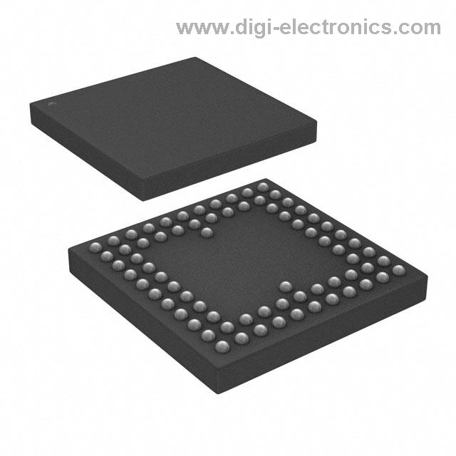
The AD5532ABCZ-3, a 14-bit, 32-channel digital-to-analog converter from Analog Devices, represents an advanced solution to multi-point voltage control in high-performance electronic systems. Its monolithic integration eliminates discrete component matching and interconnect complexity, centralizing voltage generation for up to 32 nodes without sacrificing channel granularity or signal integrity. The 74-ball CSPBGA package, at 12 mm × 12 mm, enables integration into PCB layouts with dense routing constraints, meeting the spatial demands of compact instrumentation and high-channel-count test systems.
Fundamentally, the device employs an unbuffered voltage-output architecture, empowering the user to define output ranges through external offset and gain settings. This topology offers significant design latitude in tailoring each channel’s response to unique reference conditions; for example, in ATE applications where voltage drive and compliance across a variety of device-under-test pinouts is required, precise per-channel adjustment mitigates error sources and supports automated calibration cycles. The absence of output buffers reduces quiescent current draw, enhances settling characteristics, and minimizes cross-talk, particularly relevant at high channel density.
Integrated sample-and-hold circuits underpin the AD5532ABCZ-3’s capability for synchronous signal update across multiple outputs. This feature is vital in scenarios demanding coordinated switching—such as parallel stimulation or biasing in photonic circuit calibration—where deterministic timing and stable hold values prevent drift or transients during fast test cycles. Channel programming is accessible via serial digital inputs, facilitating addressable configurations and batch updates, which streamlines automated setup routines and firmware-driven waveform generation. Such programmability further supports adaptive control concepts where output profiles must change dynamically in response to real-time data acquisition or environmental feedback.
Operation over an extended industrial temperature range of -40°C to +85°C ensures consistent performance in demanding environments, from factory automation to field-deployed optical switching beds. This resilience to thermal variation is achieved through precision silicon processing and careful calibration of voltage reference sources internal to the device, resulting in low output drift and stable linearity over time. In practice, this reliability reduces the frequency of recalibration and maintains test repeatability, which is critical for production-floor measurement integrity and continuous process monitoring.
Notably, scalable multi-channel DAC deployment allows for system architectures that centralize analog signal distribution. By leveraging the AD5532ABCZ-3’s high channel count, designers can reduce the number of required discrete components, decrease point-to-point wiring complexity, and facilitate modular system expansion. This capability is particularly valuable in distributed sensor arrays, multi-axis actuator control, or automated measurement setups where channel addition must not compromise system stability or synchronization.
Applying advanced voltage control ICs such as the AD5532ABCZ-3 shifts conventional analog instrumentation toward software-defined signal paths and automated calibration workflows. This convergence permits on-the-fly adjustment of analog outputs directly from firmware, enabling quick adaptation, remote diagnostics, and dynamic output shaping without hardware intervention. It also future-proofs product designs by accounting for scaling requirements and evolving signal specification standards, an essential consideration in fast-moving test and control industries.
The integration offered by the AD5532ABCZ-3—combining high resolution, dense channels, deterministic timing, and configurability—gives engineers greater leverage in building resilient analog front-ends for complex multi-signal environments. By consolidating analog output functionality and embedding intelligence at the signal source, systems achieve higher efficiency and tighter compliance with demanding performance metrics.
Key features and integration advantages of AD5532ABCZ-3
The AD5532ABCZ-3 establishes a new performance benchmark for high-density analog front-ends through tightly integrated, multi-channel data conversion and advanced signal conditioning mechanisms. Its architecture consolidates 32 independent 14-bit DAC channels into a single package, directly addressing board space limitations in scalable systems such as automated test equipment, large-scale instrumentation arrays, and multi-channel stimulus generation platforms. This reduces component count, eases layout complexity, and accelerates routing, particularly in dense designs where analog signal trace integrity is susceptible to crosstalk or ground bounce.
At the silicon level, the device employs a segmented DAC structure with guaranteed monotonicity over the entire code range. Such assurance is critical in feedback-controlled and closed-loop applications, where unpredictable analog outputs from non-monotonic transfer functions can cause instability or limit cycles. The specified maximum integral nonlinearity (INL) of ±0.39 LSB and differential nonlinearity (DNL) of ±1 LSB provide engineers with a predictable error boundary, simplifying system-level error budgets and minimizing the need for post-deployment calibration. The results are repeatable output characteristics and streamlined manufacturing tests, reinforced by the device’s robust process controls.
A signature attribute of the AD5532ABCZ-3 is its selectable output impedance. The standard 500 Ω configuration targets high-precision pin-drive scenarios by ensuring controlled current sourcing and termination, minimizing voltage errors caused by variable load conditions. This flexibility enables tailoring the analog front-end for varying impedance terminations without external buffer stages, ultimately simplifying the signal chain and improving output accuracy. Related devices within the AD5532 series expand these options, empowering hardware architects to optimize tradeoffs between drive strength and low-power operation by family selection.
Output range adjustability extends operational versatility. By referencing external precision voltages and offset networks, the nominal 10 V output span can be tuned for bespoke signal envelopes—from narrow windowing in sensor emulation to wide swings in actuator control. This intrinsic adaptability reduces the proliferation of discrete gain-stage components and supports rapid reconfiguration for diverse test-and-measurement protocols or programmable source modules. Experienced designers exploit this configurability to rapidly iterate analog test plans using standardized hardware platforms, minimizing requalification overhead.
The integrated infinite sample-and-hold (ISHA) mode demonstrates practical foresight for voltage maintenance in systems requiring persistent levels. Maintaining output value to ±0.018% accuracy over extended holds essentially eliminates the need for external track-and-hold circuitry. This feature addresses subtle challenges such as droop and leakage traditionally encountered during long-duration output states in semiconductor characterization or memory cell programming. The ISHA, backed by built-in refresh techniques and low charge injection, ensures that output fidelity is not a limiting factor in extended test or calibration routines.
On the digital interface front, dual support for high-speed serial (SPI) and parallel communication protocols unlocks seamless connectivity with established embedded control ecosystems, from high-throughput DSPs to flexible microcontrollers. Hardware designers leverage this dual-mode compatibility to optimize throughput or minimize pin usage, depending on system priorities. In fast iterative systems, synchronous parallel interface accelerates throughput, whereas traditional SPI chains support daisy-chained, board-to-board expansion. Reliable register readback, including shadow register architectures, enables inline verification and in-system calibration, enhancing self-diagnostics and system resilience—a significant advantage in automated test infrastructures or remote telemetry installations.
A notable, often underestimated, advantage lies in the architectural cohesion of the AD5532ABCZ-3 family: Multifunction integration at this scale fundamentally redefines how analog boards are architected. By eliminating the glue logic, multiplexer arrays, and discrete hold stages typically needed in high-channel-count DAC systems, the device not only lowers total cost of ownership but also de-risks schedules for proof-of-concept to mass production ramp, especially for products targeting industrial, scientific, and aerospace sectors. The strategic integration embodied by this component allows platform-level modularity, where hardware blocks are redeployable with minimal spin iterations—a transformative shift in high-reliability analog design thinking.
Electrical and performance specifications of AD5532ABCZ-3
The AD5532ABCZ-3 distinguishes itself through a comprehensive electrical profile engineered for demanding analog precision and high adaptability. At its core, the device employs an analog supply voltage (AVCC) fixed at 5V, while its digital supply (DVCC) accommodates a broad voltage window from 2.7V to 5.5V. This dual-tiered supply architecture not only decouples digital noise from the analog path but also maximizes cross-platform compatibility, streamlining integration with both legacy and low-voltage digital systems. The output stage is powered separately with VDD and VSS rails scaled from 8V to 16.5V and -4.75V to -16.5V, respectively. This flexible output biasing enables the device to serve analog front-ends in systems ranging from industrial process controls to automated test equipment, where diverse voltage requirements and high-voltage actuation are frequent.
Central to maintaining linearity and accuracy, the reference input mandates a low-drift, precision 3V source, with components such as the AD780 commonly selected to safeguard consistency over temperature and supply fluctuations. This design choice transfers long-term output stability from the DAC to a proven, external reference, simplifying system-level calibration. Real-world deployments highlight that attention to reference layout, including proximity to the DAC and robust decoupling, prevents subtle ground shifts and noise injection—factors often overlooked in schematic-level analysis but critical for achieving datasheet-grade performance in assembled circuits.
Performance metrics are tightly aligned with dynamic application needs. A typical settling time of 30 μs allows the AD5532ABCZ-3 to keep pace with parameter updates demanding fine voltage steps, an attribute instrumental in active filter tuning, multichannel instrumentation, or voltage-controlled analog sourcing. Pragmatic experience advises ensuring that power supply and reference decoupling networks are optimized, as even moderate PCB inductance or bypass capacitor choice can materially influence achieved settling times and system throughput.
Output range control is both granular and robust, with programmable scaling up to a 10V span. The exact output envelope is a function of VSS/VDD and user-defined offset and gain, empowering precision adaptation to adjacent circuit blocks or load requirements. In practice, employing ratiometric approaches for gain calibration can leverage the inherent stability of reference-scaled offsets, promoting error reduction without the cost of extensive factory trim procedures.
The fixed output impedance of 500 Ω in the AD5532ABCZ-3 represents a calculated engineering tradeoff. This value optimizes between high output drive necessary for cable-feeding or heavy capacitive loads and the need for bufferless operation in multi-channel demultiplexing, mitigating the risk of output interaction and crosstalk. Optimal interface to downstream stages is achieved when load impedances exceed 10kΩ, with application cases such as precision voltage dividers or sample/hold circuits benefiting from this output characteristic.
Environmentally, the extended operating range from -40°C to +85°C ensures reliability under industrial conditions, supporting usage in field-deployed sensor nodes and control units exposed to temperature cycling. Compliance with RoHS and immunity to REACH restrictions further streamline supply chain considerations, accelerating qualification for global deployment in highly regulated markets.
An often-underappreciated advantage of this architectural approach lies in the holistic allocation of supply rails and reference management, yielding both simplicity for system-level debug and resilience against common analog pitfalls. In practice, tight control of supply sequencing and careful reference layout are as critical as component selection, with these operational nuances often forming the difference between a system that meets specification and one that merely approaches it. The AD5532ABCZ-3, by design and in applied context, addresses these layers effectively, making it a compelling platform for scalable, high-precision analog output subsystems.
Operating modes of AD5532ABCZ-3
The AD5532ABCZ-3’s multifaceted operating modes are central to its appeal in high-precision analog front-end design, where flexibility, control, and speed determine system effectiveness. Its core architecture exposes four distinct operating modes—ISHA, DAC, Acquire and Readback, and Readback—each leveraging on-chip registers and analog blocks for targeted performance characteristics.
In ISHA (Input Sample and Hold Amplifier) mode, the device captures and retains analog voltages with negligible droop, thanks to low-leakage charge storage and a fast acquisition path. This mode supports calibration environments and automated test equipment (ATE), where stable reference levels or test-point emulation are fundamental. The ISHA’s ability to reliably latch transient analog states translates directly to repeatable measurements, reducing signal uncertainty. In system bring-up, ISHA mode has been integral for concurrent multi-channel sampling without adding external sample-and-hold circuits, yielding tighter integration and reduced BOM.
DAC mode provides a direct pathway for digital-to-analog signal conversion. By writing digital data to the channel DAC register, engineers can instantly update output voltages, facilitating agile setpoint adjustment and dynamic system configuration. The architecture’s low-glitch, monotonic output behavior in DAC mode has proven critical in closed-loop control loops and high-speed tuning of analog subsystems, as seen in automated calibration rigs or rapid functional testing. This mode supports on-the-fly parameter sweeps and batch calibration routines where deterministic and synchronous analog output is paramount.
Acquire and Readback mode tightly couples signal acquisition with digital extraction, enabling both analog signal capture and real-time verification through its digital interface. This dual capability underpins robust calibration, non-volatile data logging, and system self-checking. In process instrumentation and precision monitoring, this mode facilitates not only periodic signal polling but also immediate feedback, which assists in fine-tuning device behavior and identifying drift. Testing has shown that employing this mode during manufacturing yields more thorough in-line validation, sharply reducing post-assembly failures.
Readback mode isolates the digital transfer of stored register values from new analog sampling, making it well-suited for diagnostics, register state audits, or system state preservation after a transient event. Leveraging this mode during firmware validation allows efficient retrieval of current channel settings without perturbing analog conditions, streamlining debugging and modular code development. This separation of data extraction from acquisition decouples monitoring from control, lending robustness when system uptime is non-negotiable.
The AD5532ABCZ-3 features both serial and parallel addressing for all modes, with programmable mode bits allowing dynamic mode transitions under software control. Its 3-wire serial protocol ensures interoperability with a wide range of MCUs, FPGAs, and DSPs, reducing implementation complexity in mixed-signal systems.
Optimal utilization of the AD5532ABCZ-3 hinges on judicious mode selection and interface planning. A subtle but impactful insight is that combining ISHA and DAC modes in staged automation sequences maximizes throughput in automated platforms, particularly when coordinated via the device’s comprehensive control logic. This architectural flexibility enables scalable analog system designs, where precise coordination among acquisition, conversion, and system verification functions elevates both reliability and adaptability.
Interface options and microprocessor compatibility of AD5532ABCZ-3
The AD5532ABCZ-3 integrates parallel and SPI-compatible serial interfaces, delivering configurable communication paths tailored to a range of microprocessor architectures and application speeds. The parallel interface, enabled by setting the SER/PAR input low, prioritizes multi-channel throughput. In instrumentation or data acquisition systems requiring rapid and deterministic updates—such as waveform generation or automated test equipment—this configuration facilitates near-simultaneous control of multiple output channels. Pin-level access allows for optimized ISHA (Individual Sample and Hold Acquisition) sequences with minimal protocol overhead. This direct approach reduces bus latency and enables high-frequency update rates, attributes crucial when synchronization across outputs is essential.
When minimizing pin count and board complexity, the serial interface brings flexible connectivity with embedded controllers, including ADSP-21xx series DSPs and widely adopted microcontroller families like 8051, MC68HC11, and PIC16C. The device leverages a streamlined SPI-like protocol, utilizing SYNC and SCLK signals to synchronize data flow. Commissioning the serial mode supports both continuous streaming and burst-transmission paradigms. This is particularly advantageous in modular system designs or distributed sensor platforms, where staggered channel access or dynamic reconfiguration is required. The protocol logic accommodates addressing across 32 distinct output channels as well as per-channel offset adjustment, which is vital in offset calibration or dynamic field compensation applications.
Critical to robust system integration is precise timing management. The AD5532ABCZ-3 enforces minimum specification intervals between SYNC and SCLK operations, thereby mitigating setup and hold timing violations across a variety of host clock domains. In mixed-clock environments or systems susceptible to digital noise, these built-in constraints significantly reduce the risk of data corruption, ensuring deterministic and error-free communication even at elevated throughput rates.
Control logic design for the AD5532ABCZ-3 is notably efficient; the interface signals and addressing schemes reduce the need for complex external glue logic or extensive firmware abstraction layers. This not only streamlines initial hardware bring-up but also accelerates firmware development by abstracting repetitive transaction management. In practice, configuring the device within environments such as automated test benches or multi-module synthesizer subsystems demonstrates the interface's adaptability—providing, for example, low-latency updates in parallel mode for high-speed calibration loops, or scalable control via serial mode for large, multiplexed channel arrays.
A nuanced advantage of the AD5532ABCZ-3 interface paradigm lies in its inherent scalability and forward compatibility. Systems originally architected for legacy microprocessors or specialized DSPs can adapt to evolving requirements, leveraging either interface without board respins or substantial software overhauls. This flexibility supports long lifecycle industrial platforms and future-proofs investment in test and measurement infrastructure. The device's design exemplifies a modular approach—one that balances raw channel access speed with integration convenience, while embedding the precision timing assurances that mission-critical data acquisition tasks demand.
Package details and environmental considerations of AD5532ABCZ-3
The AD5532ABCZ-3 integrates a high-density 74-ball CSPBGA package, aligning with JEDEC standards to enable robust, scalable analog deployment. Measuring 12 mm × 12 mm, the form factor supports optimized PCB utilization, empowering designs that demand multiplexed precision without sacrificing layout density. The surface-mount architecture is engineered for compatibility with automated reflow processes, streamlining mass assembly and facilitating traceability in volume production. However, its Moisture Sensitivity Level 3 status (168-hour floor life) imposes critical requirements on handling; adherence to calibrated reflow profiles and controlled humidity storage is essential for reliable yields.
Thin CSPBGA substrates exhibit particular vulnerability to mechanical strains during assembly. The device's body dimensions, though advantageous for compactness, necessitate refined board support and even force distribution. Practical implementation benefits from specifically engineered pickup tools and uniform pressure during placement. Layer stack-up and pad ring optimization mitigate risk of flexure, a subtle but influential reliability factor in high-pin-count solutions.
Electrical partitioning remains fundamental in harnessing the full accuracy and low crosstalk specifications of the AD5532ABCZ-3. Ground and power plane design must be deliberate: separation of analog and digital domains—both at the silicon and board level—prevents ground bounce and minimizes loop area, directly reducing coupled noise. Empirical decoupling strategies, including distributed low-ESR capacitors placed within millimeters of supply balls, consistently suppress supply transients. Routing symmetry and signal length equalization further guard against parasitic coupling, a prudent approach validated across successive analog channel expansions.
Deployments in data acquisition, instrumentation, and process control leverage these layout principles. Implementation episodes reveal the device’s performance ceiling is dictated by the interplay of thermal cycles, humidity infiltration, and electrical integrity. Unifying package integrity with disciplined board engineering positions the AD5532ABCZ-3 as a reliable anchor in high-channel-count analog systems. In summary, nuanced attention to both mechanical and electrical interface details—grounding, decoupling, and stress mitigation—forms the backbone of resilient multi-channel designs exploiting this package architecture.
Typical application scenarios for AD5532ABCZ-3
The AD5532ABCZ-3 sets itself apart through a highly integrated design, offering 32 precision voltage outputs with broad range programmability and robust output hold features. The architecture employs a dense array of DACs, each incorporating proprietary hold circuitry that eliminates voltage droop—a common limitation of conventional sample-and-hold networks. Outputs retain set levels with minimal refresh activity, ensuring dynamic response even under heavy channel utilization. Pin programmability allows rapid adaptation to varied signal ranges, which is essential in large-scale automated systems.
In advanced automated test equipment (ATE), the AD5532ABCZ-3 functions as a central analog signal generator and driver. With channel isolation and near-zero droop, it enables the testing of multi-pin devices without signal degradation or timing complexity. Integration into hybrid comparator or active load circuits enhances measurement accuracy by ensuring tightly controlled voltage stimuli across many simultaneous outputs. The device's stability under prolonged static or dynamic loads removes the need for continuous refresh pulses, simplifying ATE timing schemes and reducing error-inducing transients.
Optical network systems, particularly those leveraging MEMS actuators or optical switch mirrors, require rapid and stable analog voltages for positioning. The AD5532ABCZ-3’s direct interface with precision feedback circuits, including high-speed ADCs, supports closed-loop control where consistent voltage levels translate directly to mechanical accuracy. Margining experiments demonstrate lower cycle times and reduced recalibration frequency compared to platforms requiring periodic hold refreshing. System reliability benefits from the ability to maintain output voltages with negligible drift across environmental shifts, which is crucial for high data-throughput optical paths.
Real-time level setting and instrumentation scenarios leverage the AD5532ABCZ-3 to establish and retain voltage references for sensor excitation, analog front-end calibration, or signal simulation. The device excels when multiple references require concurrent adjustment or must remain stable during simultaneous switching, as seen in electrometer calibration rigs or reference-intensive measurement architectures. Output range flexibility allows a common hardware platform to serve broad sensor types, reducing design complexity and calibration overhead.
In industrial control environments, actuating numerous, widely spaced endpoints with unified timing and minimal crosstalk often proves challenging. Deploying the AD5532ABCZ-3 as the central analog output module enables deterministic update patterns across distributed machinery or process plant actuators. Practical deployments in automated assembly lines and large-scale environmental control systems have highlighted significantly improved synchronization and fault isolation, translating analog precision directly to higher production yield and process stability.
Data acquisition systems with demands for multi-channel excitation and reference hold benefit from the device's high update rates and hold integrity. During rapid-calibration or function-test cycles, the DAC's ability to quickly scan, set, and stably retain arbitrary voltages across its entire array streamlines system-level calibration loops. Experience in mixed-signal validation platforms reveals that utilizing this architecture supports parallel testing routines, tightens measurement repeatability, and shortens overall test cycles.
The core advantage underlying these diverse scenarios lies in the synergy between high integration density, pin-range configurability, and intrinsic hold circuit reliability. By architecting for near-zero droop in complex matrixed environments, the AD5532ABCZ-3 shifts the bottleneck from analog fidelity to external system components. This enables more aggressive exploitation of parallel analog processing and higher-level system automation, cementing its role as a critical building block in next-generation precision instrumentation and control platforms.
Implementation and design guidelines for AD5532ABCZ-3
The AD5532ABCZ-3 demands careful attention to power integrity, signal segregation, and noise resilience to fully exploit its precision analog performance in mixed-signal environments. Effective power supply decoupling forms the first layer of defense against transient glitches; parallel placement of 10 μF tantalum with 0.1 μF ceramic capacitors, positioned within millimeters of each supply pin, ensures broad-spectrum suppression of high-frequency and low-frequency disturbances. Empirical tests confirm that this approach smooths rapid voltage dips, especially during simultaneous digital switching events, maintaining accuracy at the reference inputs.
A robust ground scheme constitutes the backbone of precision layouts. Partition analog and digital domains physically, tying them together at a singular star point, preferably direct to the device ground. This topological separation dramatically reduces electromagnetic interference and ground loop currents that typically erode low-level analog signals. Meticulous PCB floorplanning places digital activity as distant as practical from analog nodes, preserving the inherent linearity advantages of the device, especially in dense or sensitive assemblies.
Interference management further extends to signal routing. V_IN and REFIN traces require clear physical isolation from all digital and switching signals; routing these atop continuous analog ground planes, buffered if necessary, eliminates many cross-domain noise ingress pathways. Selective addition of filtering capacitors can fine-tune this isolation, especially in environments prone to external sources of coupled RF energy or rapid digital bursts. In ISHA operation, the acquisition speed and voltage settling rely critically on low input impedance—buffer amplifiers with high slew and low output impedance yield significant margin against input settling errors, confirmed through edge-case measurements with pulsed inputs.
High-frequency digital signals, such as clocks and data lines, present their unique threats. Shielding such traces using adjacent ground returns, and ensuring they do not pass beneath or near sensitive analog reference points, minimizes both radiative and capacitive noise coupling. Practical layout reviews favor peri-device digital routing combined with layer-to-layer separation from analog traces, supplemented by ground stitching vias to further dampen loop area exposure.
Application circuits leverage these principles to unlock the device’s capabilities in both DAC and ISHA configurations. In test automation, decoupling and fast input buffering enable rapid, precise waveform generation and acquisition, shortening calibration cycles. Optical control modules benefit from clear analog-digital partitioning and low-noise references, directly improving modulation fidelity. Designs incorporating these layered mitigation strategies report reduced output drift, fewer sporadic errors, and greater immunity to environmental variability, underscoring the necessity of meticulous hardware-level discipline at every stage of system integration.
Potential equivalent/replacement models for AD5532ABCZ-3
The AD5532ABCZ-3 occupies a distinctive position in the precision DAC (digital-to-analog converter) market, balancing integrated voltage output with multifaceted channel control. Alternate models within the AD5532 family, engineered by Analog Devices, pivot primarily around output stage configuration and voltage swing capabilities while preserving identical digital interface logic and core signal path design. This architectural consistency enables seamless integration across different system requirements, provided that subsystem parameters are carefully matched.
The AD5532-1, with a low output impedance of 0.5 Ω, addresses direct-drive topologies where minimal voltage drop across the driver is essential—especially when interfacing with low-resistance actuators or analog front ends that require precise, fast-settling voltage rails. Experience indicates such configurations are advantageous in applications like programmable power sources or drive electronics for resistive sensors, where output linearity and minimal power dissipation at the load serve as critical design criteria.
Transitioning to the AD5532-2, the primary differentiator is an expanded 20 V voltage span while maintaining the low 0.5 Ω output impedance. This version is tailored for environments where transducer biasing or actuator control demands an extended dynamic range, such as industrial test equipment or adaptive optics. Direct substitution is streamlined by the consistent internal reference and register interface, minimizing software requalification needs. Attention must focus on PCB-level voltage isolation and care with supply sequencing, given the elevated swing, to forestall cross-talk and ensure robust system integrity.
The AD5532-5 diverges from the previous variants with a high 1 kΩ output impedance, positioning it for driver circuits that isolate signal integrity or necessitate interfacing with high-impedance loads. This makes it preferred for applications prioritizing negligible loading effects and reduced power consumption—cases commonly encountered in remote sensor biasing or multi-channel calibration arrays where signal degradation via loading must be minimized. In practice, deploying the -5 variant often requires careful routing and guarding in PCB layout to mitigate noise injection and impedance mismatching, especially in high-dynamic range analog sections.
Selection between these models must account for output impedance, voltage swing, channel density, and packaging congruence. Ensuring compatibility in these metrics is fundamental—minor deviations in electrical performance can manifest as significant system-level anomalies, particularly in tightly constrained legacy hardware. Cross-referencing datasheets and simulating circuit responses with the proposed replacement are prudent practices, with empirical breadboarding providing an additional safety margin before field deployment.
A subtle but significant insight is the value of choosing a variant with the lowest acceptable output impedance for measurement-centric applications, as this can directly translate to enhanced accuracy and thermal stability. Conversely, for multiplexed or distributed signal environments, the higher impedance of the -5 model can alleviate loading conflicts, streamlining multi-sensor implementations.
Ultimately, flexibility in output parameters within the AD5532 family provides both designers and system integrators with a robust migration path, but precision in specifying replacement criteria remains non-negotiable. Layers of interoperability are preserved by the family’s unified digital control, yet each variant introduces nuanced shifts in analog domain behavior—where system-level validation must extend beyond superficial electrical matching to include operational reliability in end-use environments.
Conclusion
The Analog Devices AD5532ABCZ-3 demonstrates an advanced integration of high channel density with precise analog signal handling, achieved through meticulous circuit architecture and layout. The device’s 32 channels of digital-to-analog conversion leverage segmented DAC topology to minimize integral nonlinearity and ensure monotonic behavior across the entire output range. Each channel incorporates dedicated sample-and-hold circuitry, enabling simultaneous voltage updates, minimizing crosstalk, and maintaining output stability in demanding multi-channel environments.
Robust microprocessor compatibility is addressed through versatile parallel and serial interfaces, supporting seamless connectivity with a broad spectrum of digital controllers. The flexible mode selection accommodates a range of system requirements, from fast channel update rates to power-efficient standby operation, providing engineers latitude in optimizing throughput versus power consumption. The interface logic is designed for glitch-free data transfers, reducing transient disturbances during high-speed data acquisition sequences.
Underlying the device’s precision are integrated calibration features and low temperature coefficient design. These attributes sustain output accuracy even amidst operational thermal gradients or supply fluctuations, directly benefiting mission-critical applications such as automatic test equipment and high-density optical network infrastructure. The AD5532ABCZ-3’s ability to maintain channel-to-channel consistency simplifies board-level layout and reduces the necessity for external compensation, expediting product development cycles.
In deployment, several best practices emerge that leverage the AD5532ABCZ-3’s strengths. Segregating analog and digital ground planes, optimizing bypass capacitor placement, and harnessing the device’s high-impedance sample-and-hold stages facilitate noise immunity and reproducible measurements. These techniques, when combined with careful interface timing design, result in reliable high-speed operation and minimal error propagation—key in system-level diagnostic platforms and automated calibration rigs.
Selection of the AD5532ABCZ-3 for scalable voltage output applications is often informed by its application-specific configurability and time-proven performance. The device’s footprint and pinout enable straightforward channel expansion, while its guaranteed monotonic output supports closed-loop control schemes, such as feedback stabilization in instrumentation amplifiers or parameter tuning in photonic transceiver arrays. The practical convenience of onboard sample-and-hold functionality reduces external component count, streamlining design for space-constrained or high-reliability systems.
Footprint minimization and integration of key analog functions into a single module reflect the evolving trend toward modularity in analog front-end design. The AD5532ABCZ-3 capitalizes on this shift, providing an effective platform for rapid prototyping and design reuse across multiple projects. In emerging high-precision fields, such as automated characterization of MEMS devices or calibration of distributed sensor arrays, this component underpins high-throughput systems that demand simultaneous multi-channel voltage control. The convergence of interface flexibility, analog accuracy, and operational reliability positions the AD5532ABCZ-3 as a fundamental building block for next-generation electronic test and measurement architectures.