


A GTO thyristor is a high-power switch that can be turned ON and OFF using its gate. When ON, current flows from the anode to the cathode. Unlike an SCR, a GTO can be turned OFF by a negative gate current, reducing the need for extra commutation parts. This article provides information on basics, types, gate drive, switching, and protection.
GTO Thyristor Basics
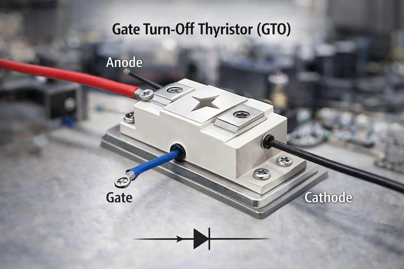
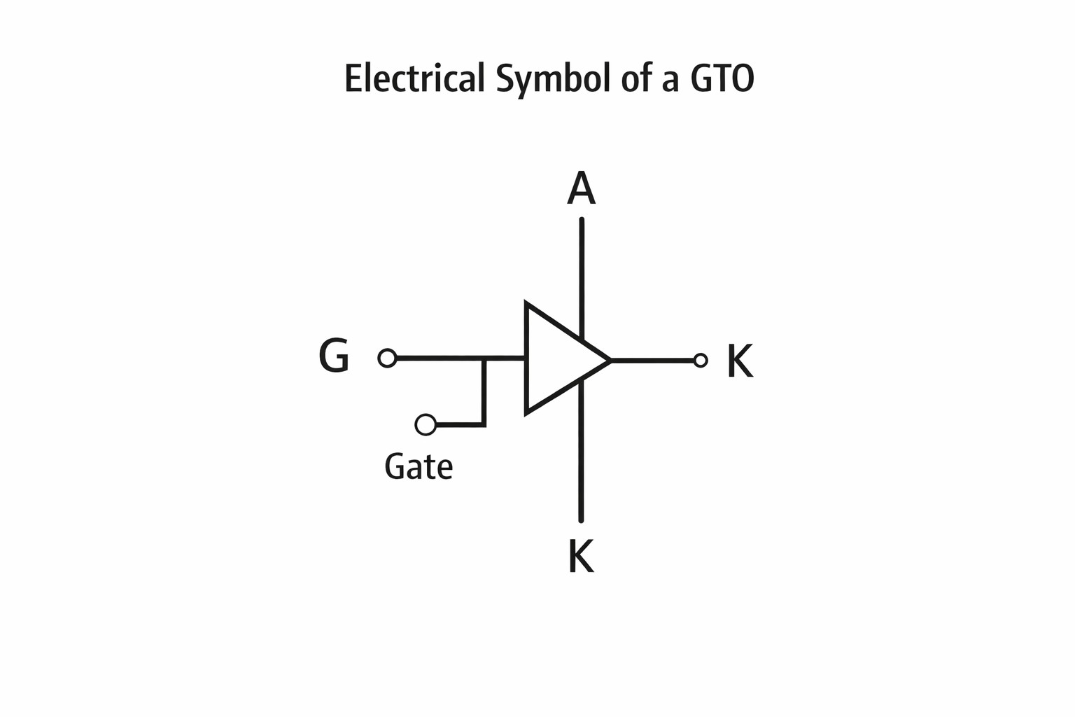
What Is a GTO Thyristor?
A gate turn-off thyristor (GTO) is a thyristor-type power switch that can be turned ON and OFF through its gate terminal. When ON, it conducts current in one direction from the anode (A) to the cathode (K). Unlike standard thyristors, a GTO can be turned OFF by a gate signal, reducing the need for external commutation circuits. It is used in applications that require high current and voltage handling.
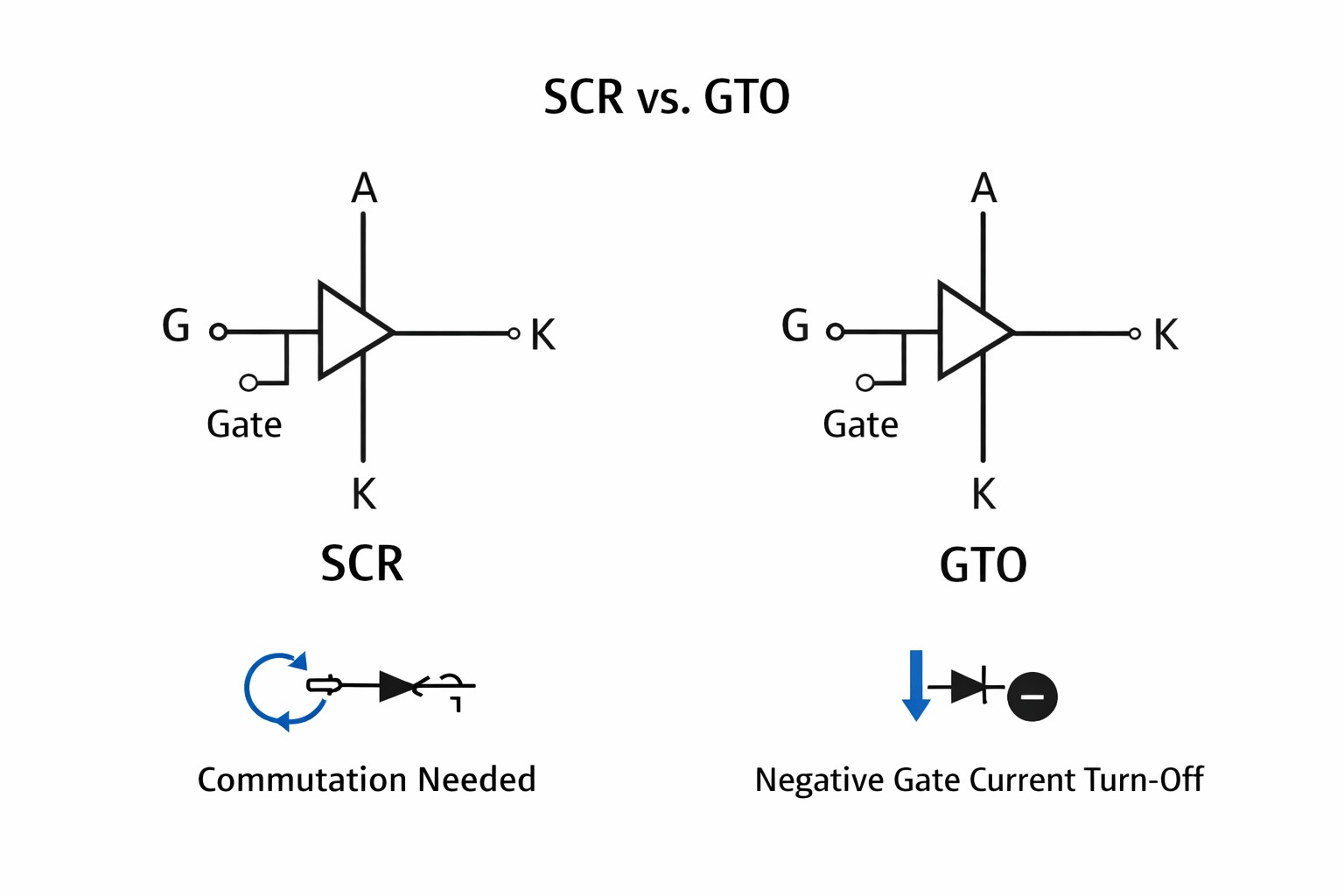
GTO vs SCR in Circuit Control
Feature Comparison Table
| Feature | SCR (Conventional Thyristor) | GTO Thyristor |
|---|---|---|
| Turn ON | Gate pulse | Gate pulse |
| Turn OFF | Needs commutation or current forced below holding current | Negative gate current turns it OFF |
| Control level | Semi-controlled | Fully controlled (gate controls ON and OFF) |
| Circuit impact | Extra commutation parts are often needed | Less dependence on commutation, but a strong gate drive is needed |
Commutation Impact in Actual Converters
An SCR keeps conducting after it is turned ON until the circuit forces the current down below its holding level. Because of this, many SCR circuits require additional commutation components or specific circuit timing to turn the device OFF. This can make the converter larger and more complex.
A GTO can be commanded to turn OFF through the gate, so the circuit does not always need the same commutation networks. Turning a GTO OFF is not free. The gate driver must deliver a high-peak gate current for turn-off, and the timing must be carefully controlled to avoid device stress.
Internal Construction of a GTO
PNPN Structure and Junction Behavior
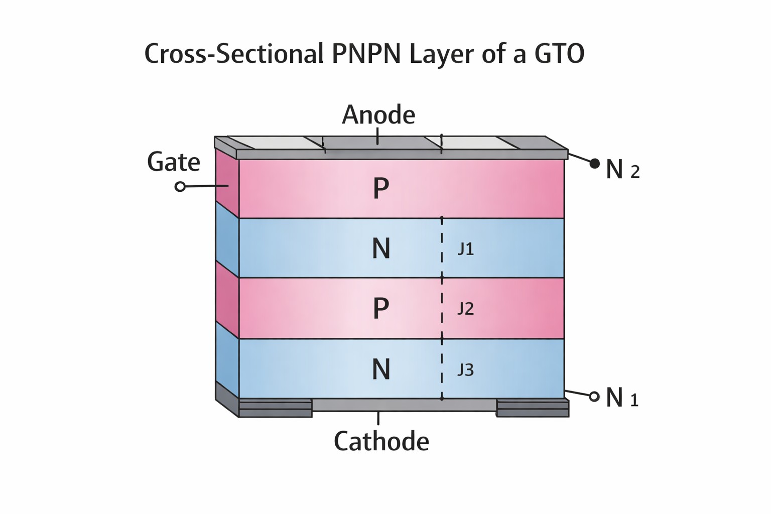
Inside, a GTO is built as a four-layer PNPN device with three junctions (J1, J2, and J3), similar to an SCR. When a turn-on signal is applied at the gate, the device begins to conduct and then latches ON, meaning it can stay ON even after the gate signal is removed, as long as current continues to flow in the forward direction.
A difference is that the GTO is made so the gate can also help turn it OFF. During turn-off, the gate is driven to remove charge carriers from the device. With fewer charge carriers available, the internal mechanism that keeps the GTO latched weakens, and conduction can stop.
Cellular Design and Current Sharing
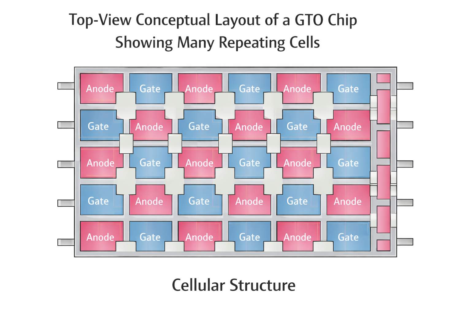
Most GTOs are not made as a single large switching area. Instead, they use a cellular structure, which means the chip is divided into many small thyristor cells connected in parallel. This layout helps the current spread more evenly across the device, rather than concentrating in one spot.
When current is shared more evenly, switching is more stable, and the device is less likely to have small areas that heat much more than others. This supports smoother turn-on and turn-off when handling large currents.
GTO Operating States in Converters
Forward Blocking State
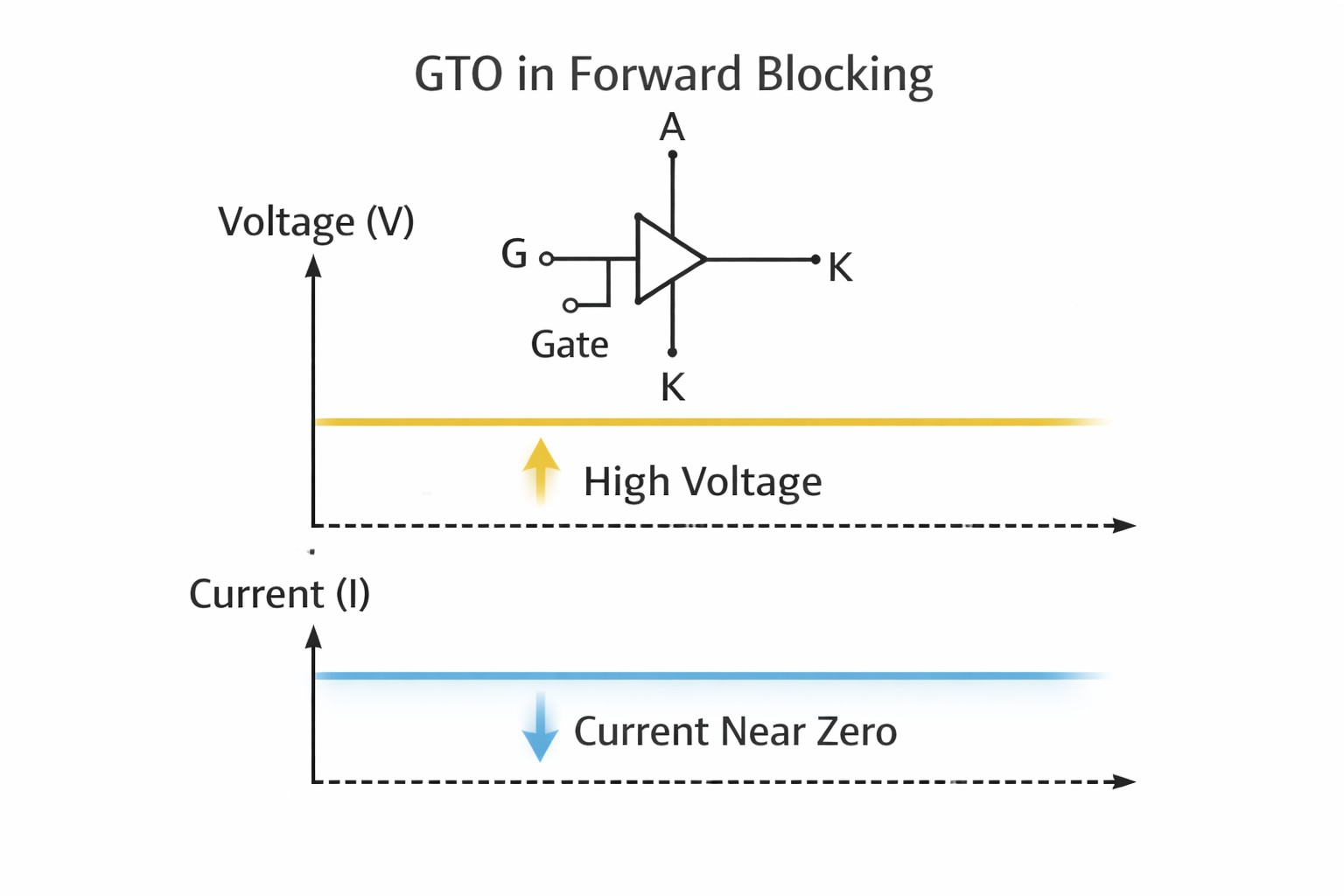
In the forward-blocking state, the GTO is OFF, but a forward voltage is applied across it. The device holds back that voltage, so the primary current does not flow. Only a tiny leakage current may pass through the device when it is blocking, which is normal. The main points: Blocks forward voltage while OFF, and only leakage current flows.
Forward Conduction State
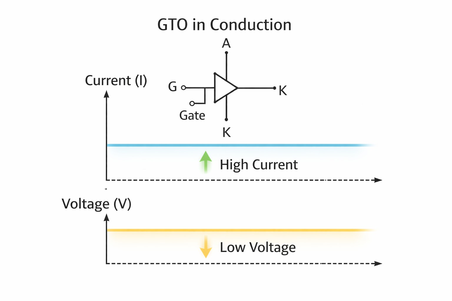
In the forward conduction state, the GTO is ON and carries the main load current from anode to cathode. The voltage across the device becomes much lower than in the blocking state, but it does not drop to zero. This remaining voltage is the on-state drop, and it causes conduction loss while the GTO is carrying current.
Reverse Behavior
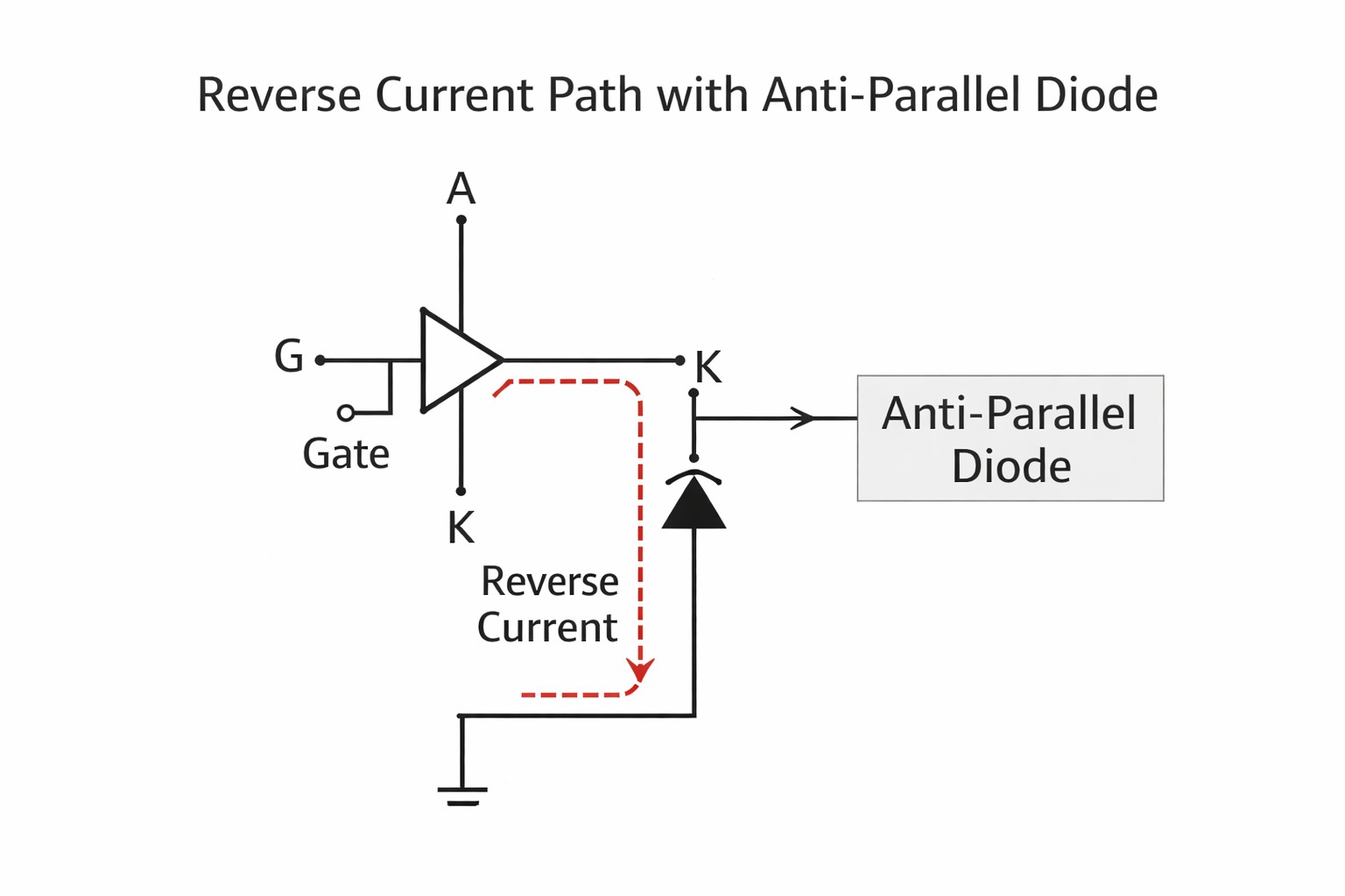
Reverse behavior depends on the device type. A symmetric GTO can block voltage in both directions, so it may handle reverse blocking without an added path. An asymmetric GTO is intended to block forward voltage, so reverse current is dealt with by an anti-parallel diode connected across the device.
Gate Control and Switching Behavior in a GTO
Gate Control Basics: +Ig for ON, −Ig for OFF
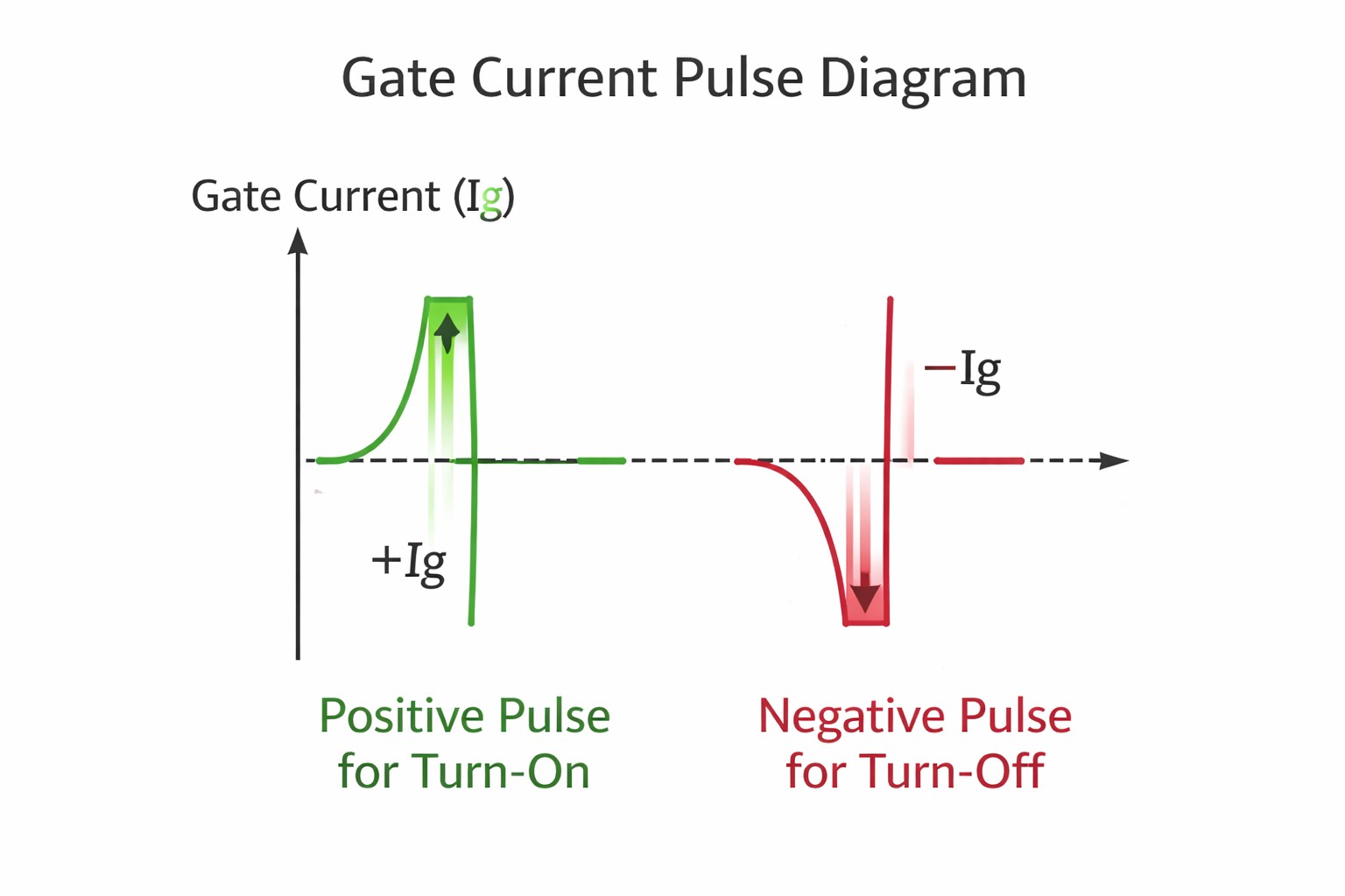
A GTO gate is current-driven, not voltage-driven. To turn the device ON, a positive gate current is applied from the gate (G) to the cathode (K). This starts conduction inside the PNPN structure, and the device can latch into the ON state.
To turn the device OFF, a negative gate current is applied. This negative current helps pull charge carriers out of the device, thereby stopping conduction. Turn-off is not done with a small signal. It needs a large peak negative gate current for a short time to force the device out of conduction.
Turn-ON Process: Current Spreading and di/dt Control
When a GTO begins turning ON, conduction starts near the gate area and then spreads across the rest of the device. If the current rises too fast, the first conducting areas may carry too much current before the rest of the chip entirely turns on. This can cause uneven heating and stress, so the rate of rise of current (di/dt) is often controlled.
A series inductance or a saturable reactor may be used to slow the current rise. The gate current can also be shaped to allow turn-on to spread more smoothly across the device. A low-inductance power path helps reduce unwanted spikes and supports more even current flow during the switching transition.
Turn-OFF Process: Carrier Extraction and Tail Current
Turning OFF a GTO uses negative gate current to remove charge carriers stored inside the device. Even after the turn-off command is applied, the current may not drop to zero right away. Many GTOs exhibit a tail current, in which a smaller current persists for a short time as the remaining charge clears. This tail current increases switching losses and affects the voltage control required during turn-off.
Turn-off loss rises because current can still be present while the device voltage increases. dv/dt stress can also be higher during this period. Because tail current takes time to disappear, it limits how quickly the device can switch repeatedly.
Switching Frequency Limits
GTOs are limited to low kHz switching, depending on the device rating and circuit conditions. Charge storage and tail current increase switching losses, so the frequency is often set by heat and loss limits rather than by control speed alone.
Electrical Behavior of a GTO
V–I Curve: Latching and Blocking Region
A GTO behaves much like a standard thyristor when you look at its voltage–current (V–I) curve. In the OFF state, it can block a forward voltage, and only a small leakage current flows. When it is triggered ON, it enters conduction, and the current increases while the voltage across the device drops to a much lower level.
After it latches ON, the GTO will keep conducting as long as the main current stays above its holding level. Unlike an SCR, a GTO can be pushed back toward the blocking state by applying a negative gate current. This turn-off action has limits, since the device needs enough negative gate current and proper conditions to stop conduction safely.
Conduction Loss Basics
| Parameter | What does it tell you? | Why does it matter? |
|---|---|---|
| On-state voltage drop (V_ON) | Voltage across the device while ON | Higher V_ON means more heat |
| Load current (I) | Current through the device | The higher I is, the more dissipation |
| Conduction loss | Approx. V_ON × I | Affects heat removal needs |
Common GTO Types and Circuit Effects
GTO Types
| Type | Reverse Blocking | Typical Use |
|---|---|---|
| Symmetric (S-GTO) | High reverse blocking | Current-source style designs |
| Asymmetric (A-GTO) | Low reverse blocking | Voltage-source inverters (with a diode) |
| Reverse-Conducting (RC-GTO) | Integrated diode | Compact inverter modules |
Selection Notes
• If a reverse current path exists, include a diode solution, either external or integrated
• Match the reverse blocking ability to the converter’s topology and expected voltage direction
• Consider whether the needed device type is available in a suitable package or module for the required power level
Gate Driver Needs for a GTO
High Peak Gate Current Requirements
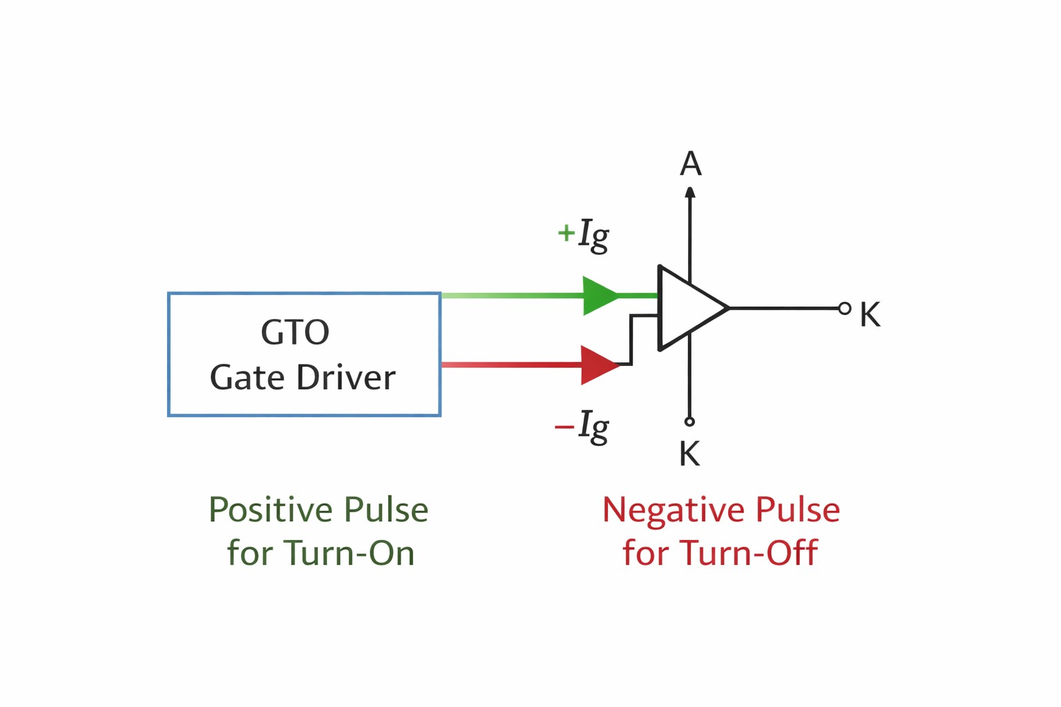
A GTO gate driver must supply current in both directions because the gate controls turn on and off. For turn-on, it delivers a strong positive gate current to start conduction quickly and help the device turn on evenly. For turn-off, it delivers a strong negative gate current to pull charge carriers out of the device, stopping the current.
Pulse timing and pulse length matter because the device needs enough gate current for long enough to complete the switching action. If the turn-off pulse is too weak or too short, the device may not fully turn off, leaving it in a stressed, unstable state.
Low-Inductance Layout and Pulse Shaping
Low inductance in the gate path is basic because inductance opposes rapid current changes. If the loop inductance is high, gate current transitions become slower, leading to unwanted voltage spikes. This can lead to uneven switching and local heating during turn-on or turn-off. A tight, low-inductance layout helps the gate pulses reach the device cleanly, and pulse shaping can further smooth the current rise and fall.
Protection and Safe Switching for GTOs
| Risk | What happens | Solution |
|---|---|---|
| High di/dt at turn-on | Current can crowd into small areas and cause overheating | Series inductance, gate shaping |
| High dv/dt at turn-off | Voltage spikes can appear while the tail current is still flowing | RC snubber, clamp networks |
| SOA violation | Combined current, voltage, and time stress exceeds device limits | Coordinated gate drive and protection |
Guide for Using GTOs
Advantages and Disadvantages of GTOs
| Advantages | Disadvantages |
|---|---|
| Gate-controlled turn-off reduces commutation dependence | A large gate current is required, especially for turn-off |
| Handles very high voltage and current | Tail current increases losses and limits switching frequency |
| Established performance in high-power conversion | Protection networks add circuit complexity |
Applications Where GTOs Fit
• Traction and rail drives
• Heavy industrial motor drives
• High-power inverters and choppers
Modern Alternatives
| Device | Why is it used? | Advantage vs GTO |
|---|---|---|
| IGCT | High-power switching in the thyristor family | Faster and more efficient turn-off |
| IGBT | Common choice for many inverter designs | Voltage-driven gate and higher switching frequency |
Conclusion
GTOs handle very high voltage and current, but their limits shape converter design. Turn-on must control di/dt so current spreads evenly. Turn-off needs a large negative gate pulse, and tail current raises loss and dv/dt stress, which keeps switching in the low kHz range. Reverse behaviour depends on type: symmetric blocks in both directions, asymmetric requires an anti-parallel diode, and RC-GTO includes a diode for reverse current.
Frequently Asked Questions [FAQ]
What gate voltage drives a GTO?
Enough voltage to force the required gate current (+Ig and −Ig).
How do you confirm a GTO is ON?
Anode–cathode voltage is low while the main current is flowing.
How do you confirm a GTO is OFF?
The primary current is near zero while the device holds the blocking voltage.
Why keep the gate lead short?
To reduce inductance and ringing, keep the gate pulse clean.
What is turn-off re-triggering?
The GTO turns back ON after a turn-off command due to high dv/dt or gate noise.
What sets the practical switching frequency limit?
Thermal limit from conduction and turn-off losses, tail current loss.


