


Castellated holes are plated half-holes on the edge of a PCB that let one board solder flat onto another with a low profile. This article explains what they are, how they compare with other connection options, and where they are used. It also covers how they are made, key size rules, surface finishes, board thickness, and edge quality, assembly on a carrier board, electrical layout, and typical faults.
Castellated Holes Overview
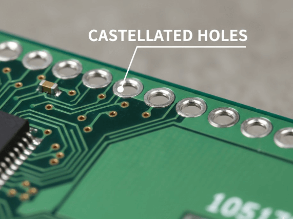
Castellated holes, also called plated half-holes or castellations, are plated through-holes placed along the edge of a PCB and then cut in half when the board outline is routed. This creates a row of plated half-circles on the board edge. These features solder to matching pads on another PCB, allowing a small board to mount directly to a larger board with a low-profile, soldered connection.
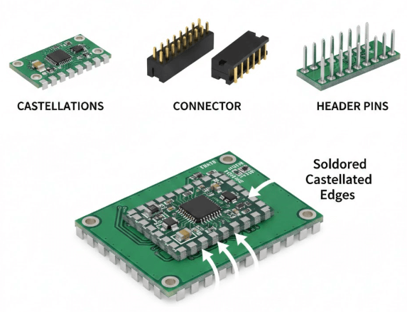
Castellated Holes Among PCB Interconnect Options
| Interconnect option | Best suited for | Key trade-offs |
|---|---|---|
| Castellated holes | Compact solder-down PCB modules | Not a plug-in interface; requires soldering |
| Board connectors | Connections that need to be unplugged often | Adds height, cost, and extra component count |
| Header pins | Simple or temporary PCB connections | Taller, less rigid, and more manual assembly |
Common Application for Castellated Holes
• Compact wireless modules soldered onto a main board
• Small IoT and sensor boards mounted on a base PCB
• Daughterboards stacked on a main board where height is limited
• Breakout boards are designed to solder directly to a larger PCB
Castellated Hole Manufacturing Process
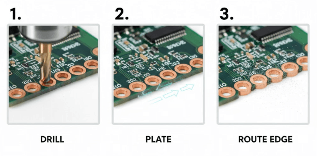
• Drill a straight row of through-holes close to the edge of the PCB.
• Plate these holes with copper during the normal plated through-hole process.
• Route or mill the board outline so the cut passes through the center of each hole, leaving plated half-holes along the edge.
Castellation Geometry and Pad Design Rules
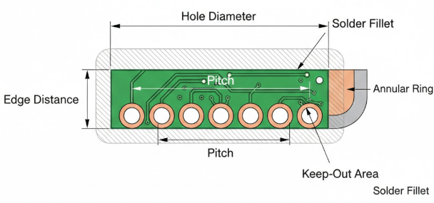
| Term | What it means | Practical starting point |
|---|---|---|
| Finished hole diameter | Hole size after plating is complete | ≥ 0.5 mm |
| Hole-to-hole spacing | The gap between the centers of adjacent holes | ≥ 0.5 mm |
| Edge clearance | Distance from copper or features to the routed edge | Follow PCB fab rules; tighter values increase risk and cost |
| Keep-out | Area kept clear of copper or sensitive features | Match routing tolerance and allow room for inspection |
| Annular ring | A copper ring around the plated hole | Often 0.25–0.30 mm (or more), depending on fab capability |
Board Thickness, Edge Quality, and Castellation Strength
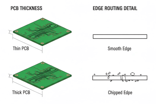
Because castellated holes sit on a routed edge, both edge quality and board thickness affect chipping, burrs, and damage during handling. Thicker boards can handle more stress, while thinner boards can still work well if depaneling and assembly are controlled. It helps to plan how modules will be separated, packed, and placed so the castellated edge is protected from impact and bending.
Carrier Footprints and Assembly for Castellated Holes
Many issues with castellated holes show up on the carrier footprint, such as solder bridges on tight pitch, weak fillets, or slight misalignment. The castellation row behaves much like a row of SMT edge pads, so the carrier layout and paste delivery should be tuned for stable, repeatable solder joints.
Carrier Footprint and Paste Control
• Align carrier pads closely to the castellated row with clear solder mask definition
• Use solder mask dams on tight pitch to limit solder bridging
• Adjust stencil apertures if paste builds up at the edge or bridges appear
• Add alignment aids such as silk outlines, courtyards, and fiducials
Assembly Method Choices
| Method | Good for | What to watch |
|---|---|---|
| Reflow | Production builds | Paste volume and bridges on a tight pitch |
| Hand solder | Prototypes, small runs | Uneven fillets and overheating |
| Hot-air rework | Repair or replacement | Pad lifting from excess heat |
Rework Tips
• Use flux and controlled heat to avoid dull or weak joints
• Inspect both ends of the castellation row, since bridges can start at the corners
• Shield nearby parts and lift the module gently rather than prying it up
Electrical Layout for Castellated Hole Connections
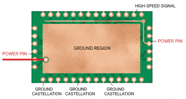
• Use several ground castellations to lower return path impedance and strengthen the row
• Spread higher-current pins along the edge instead of grouping them near one corner
• Keep fast signal lines short across the interface and reference them to a solid ground area
• Route noise-sensitive signals away from corners that see more bending and mechanical stress
Castellated Hole Failures and Solutions
| Failure mode | What it looks like | How to reduce it |
|---|---|---|
| Solder bridging | Shorts between nearby castellated pads | Use solder mask dams, control paste volume, and match pad pitch |
| Weak fillet/opens | Thin or patchy solder, unstable connection | Improve land pattern, use enough flux, tune reflow profile |
| Edge burrs / chipping | Rough or chipped board edge near pads | Tight routing controls, careful depaneling, and packaging |
| Plating breakout | Damaged or missing copper at the cut edge | Use enough annular rings and confirm the factory's capability |
Conclusion
Castellated holes form a compact, soldered link between boards when their details are planned as one system. Suitable dimensions, clear fabrication notes, and a stable surface finish support solid joints at the edge. Matching the carrier footprint, paste amount, and assembly method to the castellation row, along with careful layout and inspection, helps limit bridging, edge damage, and plating defects.
Frequently Asked Questions [FAQ]
Can I use castellated holes on multilayer PCBs?
Yes. You can use them on multilayer boards, but pull back inner copper planes from the castellated edge to avoid unwanted connections.
How much current can a castellated pin carry?
It depends on copper thickness, pad size, and how many pins share the net. For higher current, use thicker copper, larger pads, and several castellated pins in parallel.
Are castellated holes okay for RF or high-speed signals?
Yes. Keep traces short, give them a solid ground reference, and avoid sudden changes in trace width near the castellations.
How do castellated holes affect panelization and depaneling?
They often work better with tab routing than V-scoring. Place break lines so the separation step does not chip the plated edge or crack the copper.
Can a castellated module go through more than one reflow cycle?
Yes. Make sure the reflow profile stays within the rated peak temperature and time above liquidus for the PCB material and components.


